Epitaxial structure of light emitting diode and preparation method thereof

A technology of light-emitting diodes and epitaxial structures, applied in the field of diodes, can solve the problems of lattice mismatch, poor crystal quality of epitaxial layers, etc.

Active Publication Date: 2022-04-12
JIANGXI ZHAO CHI SEMICON CO LTD
View PDF7 Cites 0 Cited by
  • Summary
  • Abstract
  • Description
  • Claims
  • Application Information

AI Technical Summary

Problems solved by technology

[0006] Aiming at the deficiencies of the prior art, the object of the present invention is to provide an epitaxial structure of a light-emitting diode and its preparation method, aiming at solving the lattice mismatch in the prior art, resulting in poor crystal quality of the epitaxial layer for subsequent epitaxial growth question

Method used


Image

  • Epitaxial structure of light emitting diode and preparation method thereof
  • Epitaxial structure of light emitting diode and preparation method thereof
  • Epitaxial structure of light emitting diode and preparation method thereof

Examples


Embodiment 1

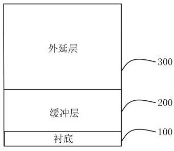
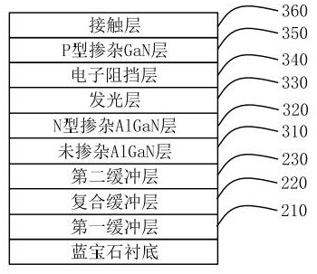
[0034] see Figure 1-Figure 2 , shows an epitaxial structure of a light emitting diode provided in the first embodiment of the present invention, which is applied to a micro light emitting diode or an ultraviolet light emitting diode. The epitaxial structure of a light emitting diode includes: a substrate 100, a buffer layer 200 and an epitaxial layer 300; , the substrate 100 is a substrate for subsequent growth of the epitaxial layer 300 , and is used to support and fix the subsequent growth of the epitaxial layer 300 . Among them, the material of the substrate 100 is the cornerstone of technological development in the field of lighting, and is the main factor determining the performance indicators such as the color, brightness, and life of the light-emitting diode. The packaging technology of the light emitting diode, and therefore the choice of the material of the substrate 100 determines the development route of the light emitting diode. The material of the substrate 100 ...

Embodiment 2

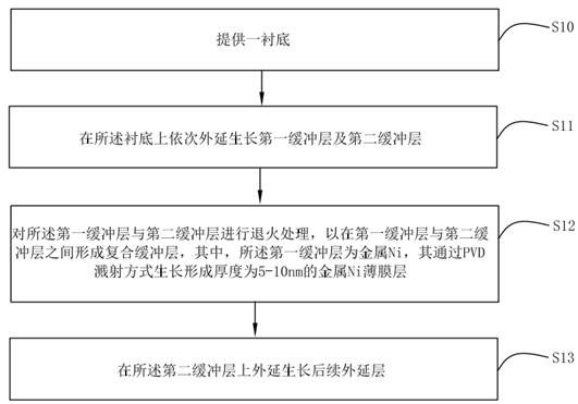
[0050] see image 3 , which shows a method for manufacturing a light-emitting diode provided in the second embodiment of the present invention, the method includes steps S10-S13:

[0051] Step S10, providing a substrate;

[0052]Among them, the crystal structure of the substrate material and the epitaxial material must be the same or similar, and the lattice constant mismatch degree is small, otherwise the growth quality of the subsequent epitaxial layer will be affected. In this embodiment, (0001) crystal orientation sapphire (Al 2 o 3 ) as a substrate, the chemical performance of the sapphire substrate is stable, and the structure of the sapphire substrate will not be damaged during the growth process of the subsequent epitaxial layer after high temperature growth. At the same time, the sapphire substrate does not absorb visible light, the price is moderate, and the preparation is simple.

[0053] Step S11, epitaxially growing a first buffer layer and a second buffer layer...


PUM

PropertyMeasurementUnit
thicknessaaaaaaaaaa
thicknessaaaaaaaaaa
thicknessaaaaaaaaaa

Abstract

The invention provides an epitaxial structure of a light-emitting diode and a preparation method of the epitaxial structure, relates to the technical field of diodes, and is applied to a miniature light-emitting diode or an ultraviolet light-emitting diode. The epitaxial structure of the light-emitting diode comprises a substrate, a buffer layer and an epitaxial layer; the buffer layer is arranged between the substrate and the epitaxial layer, the buffer layer sequentially comprises a first buffer layer, a composite buffer layer and a second buffer layer, the first buffer layer is arranged on the substrate, the first buffer layer is made of metal Ni, and the first buffer layer grows in a PVD sputtering mode to form a metal Ni thin film layer with the thickness of 5-10 nm. According to the invention, the technical problem of poor crystal quality of an epitaxial layer of subsequent epitaxial growth caused by lattice mismatch generally existing in a light-emitting diode in the prior art can be solved.

Description

technical field [0001] The invention relates to the technical field of diodes, in particular to an epitaxial structure of a light emitting diode and a preparation method thereof. Background technique [0002] With the continuous progress and development of science and technology, light-emitting diodes have been widely used in displays and lighting. Light-emitting diodes (LEDs) release energy through the recombination of electrons and holes to emit light, which converts electrical energy into light energy to achieve light emission. The light-emitting diodes, the industrial mass production of light-emitting diodes are mainly blue-green light-emitting diodes. As people have higher and higher requirements for the display brightness, contrast and resolution of light-emitting diodes, micro-diodes and ultraviolet diodes are highly concerned. The pixel distance is reduced from the millimeter level to the micron level, which shows great advantages in terms of brightness, contrast an...

Claims


Application Information

Patent Timeline
Patent Type & Authority Applications(China)
IPC IPC(8): H01L33/12H01L33/00C23C14/18C23C14/16
Inventor 胡加辉刘春杨吕蒙普金从龙顾伟
Owner JIANGXI ZHAO CHI SEMICON CO LTD
Why Eureka
Try Eureka