A kind of epitaxial growth method of high crystal quality infrared light-emitting diode
A technology of epitaxial growth and crystal quality, which is applied in the direction of semiconductor devices, electrical components, circuits, etc., can solve the problems of poor crystal quality in epitaxial layers, and achieve the effects of improving crystal quality, increasing internal quantum luminous efficiency, and increasing luminous efficiency
- Summary
- Abstract
- Description
- Claims
- Application Information
AI Technical Summary
Problems solved by technology
Method used
Image
Examples
Embodiment 1
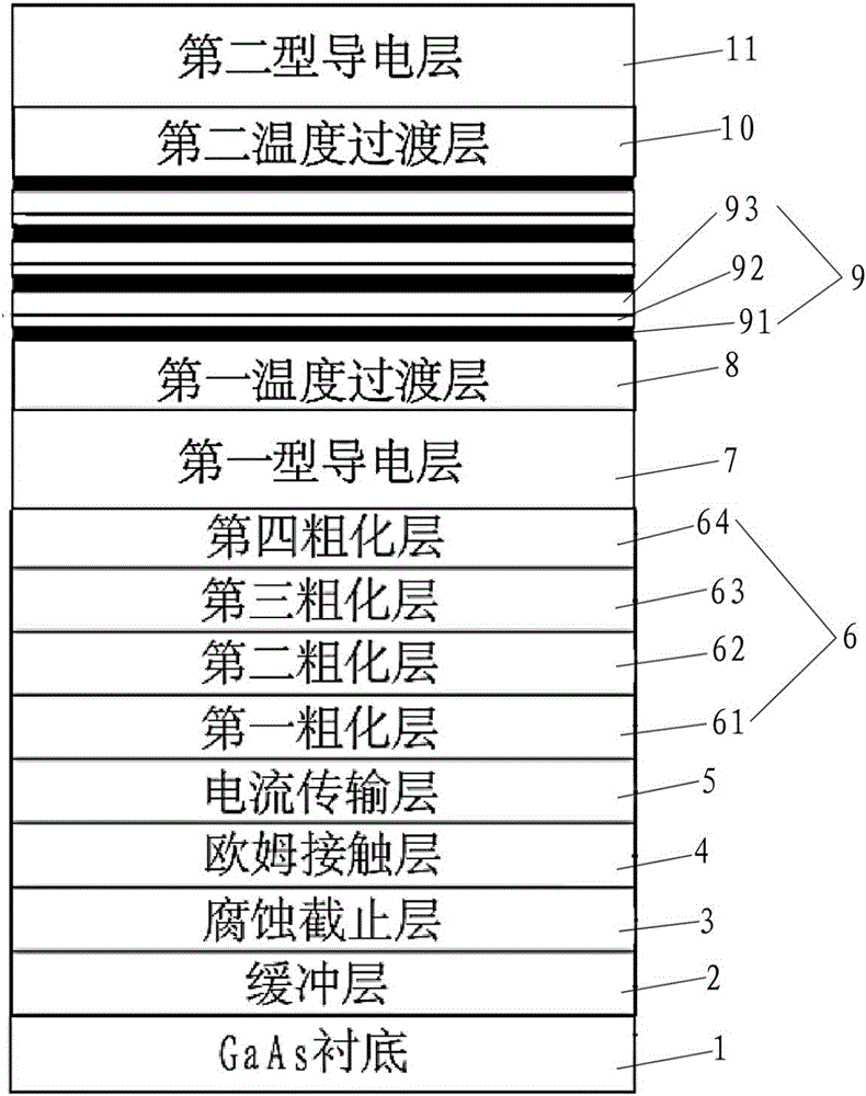
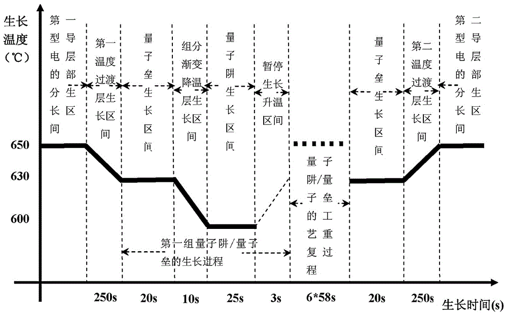
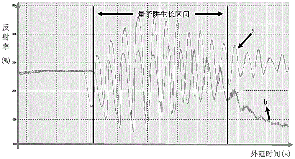
[0066] Refer to Figure 1 to Figure 4 As shown, a high-crystalline quality infrared light-emitting diode disclosed by the present invention, from the substrate 1 to the bottom-up in sequence is the growth buffer layer 2, the corrosion stop layer 3, the ohmic contact layer 4, the current transport layer 5, and the roughened layer 6. , The first type conductive layer 7, the first temperature transition layer 8, the active layer 9, the second temperature transition layer 10, and the second type conductive layer 11.
[0067] The roughened layer 6 is composed of four parts, which are a first roughened layer 61, a second roughened layer 62, a third roughened layer 63, and a fourth roughened layer 64, respectively.
[0068] The active layer 9 is alternately composed of seven sets of quantum barriers 91, a temperature-graded cooling layer 92 and quantum wells 93.
[0069] A method for epitaxial growth of high crystal quality infrared light emitting diodes, the specific steps are as follows:...
Embodiment 2
[0089] The difference between the second embodiment and the first embodiment is that the active layer 9 is composed of six sets of quantum barriers 91, the composition gradient cooling layer 92 and the quantum wells 93 alternately, while the first embodiment has seven sets.
[0090] Such as Figure 5 As shown, an infrared light-emitting diode, from substrate 1 to bottom to top, is the growth buffer layer 2, the corrosion stop layer 3, the ohmic contact layer 4, the current transport layer 5, the roughened layer 6, and the first type conductive layer 7. , The first temperature transition layer 8, the active layer 9, the second temperature transition layer 10, and the second type conductive layer 11.
[0091] The roughened layer 6 is composed of four parts, namely the first roughened layer 61, the second roughened layer 62, the third roughened layer 63, and the fourth roughened layer 64; the active layer 9 consists of six sets of quantum barriers 91, The composition gradient cooling ...
PUM
 Abstract
Description
Claims
Application Information


