
Storage unit and storage array erasing method

A storage unit and storage array technology, applied in the field of memory, can solve problems such as low memory durability, and achieve the effects of increasing read current, increasing voltage difference, and improving durability

Active Publication Date: 2014-12-03
SHANGHAI HUAHONG GRACE SEMICON MFG CORP
View PDF4 Cites 5 Cited by
  • Summary
  • Abstract
  • Description
  • Claims
  • Application Information

AI Technical Summary

Problems solved by technology

[0013] The present invention solves the problem of low memory durability

Method used


Image

  • Storage unit and storage array erasing method
  • Storage unit and storage array erasing method
  • Storage unit and storage array erasing method

Examples


Embodiment Construction

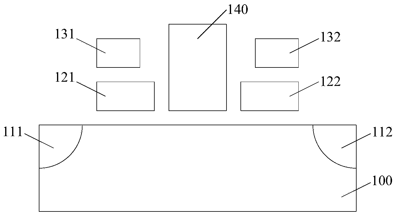
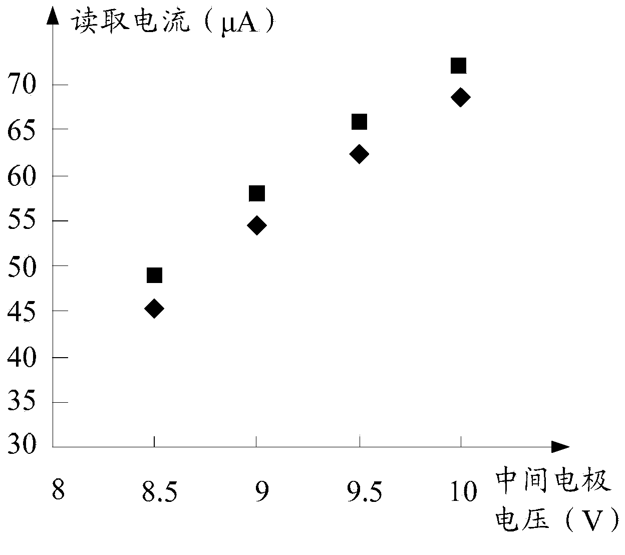
[0053] Endurance is an important index to measure the reliability of the memory, which means that the read current of the memory still meets the requirements after multiple erasing operations. for figure 1 For the shown memory cell, the magnitude of the read current after the erase operation is related to the applied erase voltage. for research figure 1 The specific relationship between the read current of the shown memory cell and the applied erasing voltage, the inventor adopts the erasing method of the prior art to figure 1 The memory cells shown were verified twice.

[0054] When verifying for the first time, multiple erasing operations are performed on the memory cell, and in each erasing operation, the voltage applied to the P-type well region 100 is the same, and the voltage applied to the drain 111 is the same, The voltage applied to the source 112 is the same, the voltage applied to the first control gate 131 is the same, the voltage applied to the second control g...


PUM


Abstract

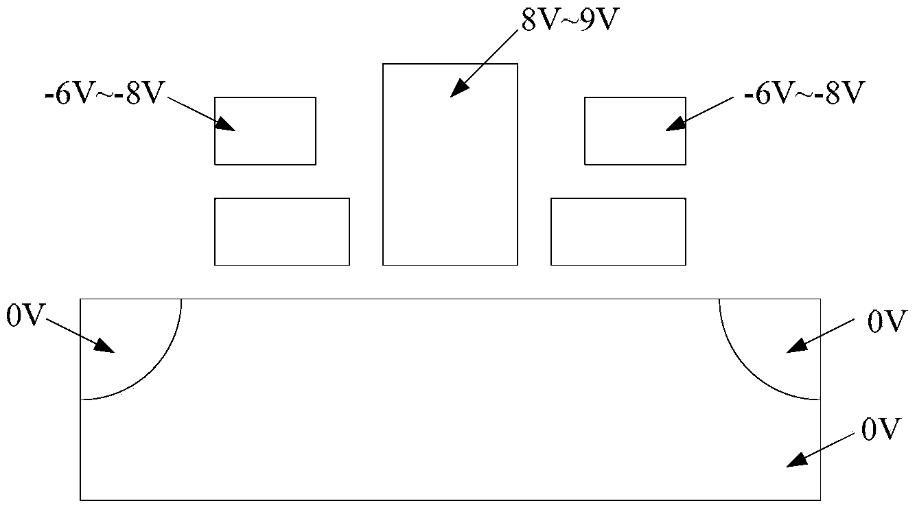
The invention relates to a storage unit and a storage array erasing method. The storage unit comprises a P-type well region, a drain electrode, a source electrode, a first control grid electrode, a second control grid electrode and a middle electrode; the storage array erasing method comprises the following steps: applying first bias voltage to the P-type well region; applying second bias voltage to the drain electrode; applying third bias voltage to the source electrode; applying minus 6V-minus 8V voltage to the first control grid electrode; applying minus 6V-minus 8V voltage to the second control grid electrode; and applying 8V-9V voltage to the middle electrode, wherein the value of the first bias voltage is negative, and the values of the first bias voltage, the second first bias voltage and the third first bias voltage are equal. The storage unit and the storage array erasing method can improve the durability of the storage unit.

Description

technical field [0001] The invention relates to the technical field of memory, in particular to a method for erasing a memory unit and a memory array. Background technique [0002] Non-volatile memory (NVM, Non-volatile Memory) refers to a memory whose stored data will not disappear after power failure. Generally, non-volatile memory includes erasable and writable read only memory (EPROM), electrically erasable and writable read only memory (EEPROM), and flash memory. There are currently two basic types of non-volatile memory cell structures: stacked gate and split gate structures, in which split gate memory cells are obtained because they can effectively avoid the over-erasing effect and have higher programming efficiency. widely used. [0003] figure 1 It is a schematic cross-sectional structure diagram of an existing double split gate memory cell. The memory cell includes: a P-type well region 100 located in a semiconductor substrate; an intermediate electrode 140 loc...

Claims


Application Information

Patent Timeline
IPC IPC(8): G11C16/14
Inventor 胡剑杨光军
Owner SHANGHAI HUAHONG GRACE SEMICON MFG CORP
Learn More