A method for determining the boundaries of wafer test data specifications and a method for marking die
A technology of wafer testing and data specification, which is applied in the semiconductor field, can solve problems such as unsatisfactory, discarding, and improving, and achieve the effects of reducing the probability of error, improving production efficiency, and reducing waste
- Summary
- Abstract
- Description
- Claims
- Application Information
AI Technical Summary
Problems solved by technology
Method used
Image
Examples
Embodiment 1
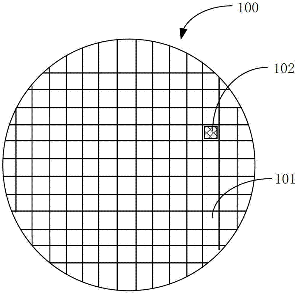
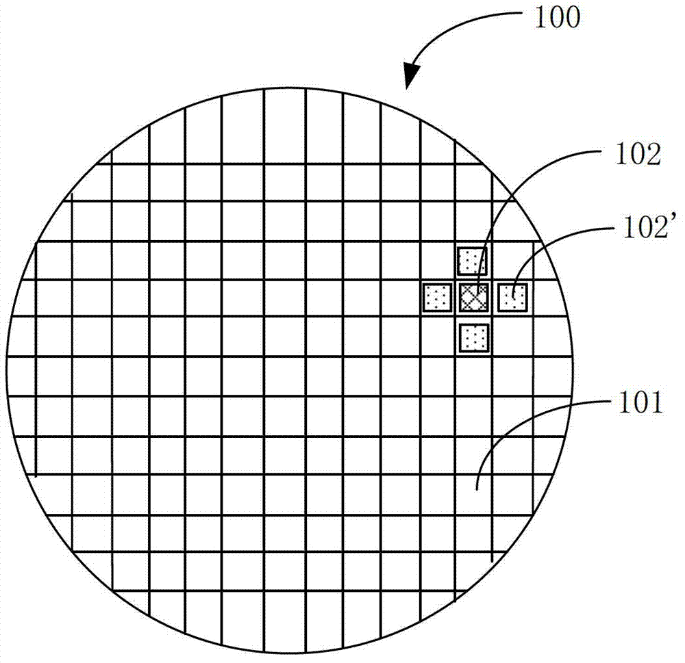
[0035] This embodiment provides a method for determining the limits of wafer test data specifications, wherein the method determines corresponding limits of wafer test data specifications for different wafers. That is to say, this embodiment adopts a method of dynamically determining the limit of the wafer test data specification to determine the limit of the wafer test data specification, which is different from the method of statically determining the limit of the wafer test data specification in the prior art. (That is, the method of using the same wafer test data specification for all wafers) is obviously different, which is conducive to improving the yield of the die on the wafer.
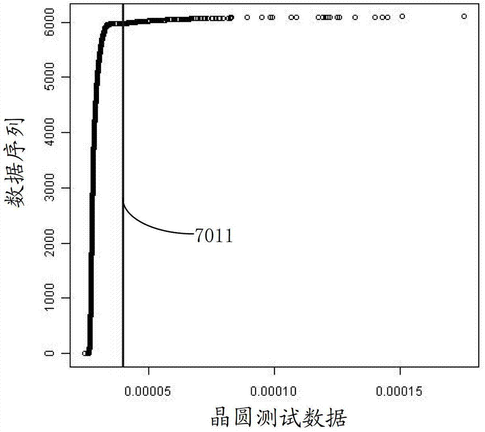
[0036] For ease of understanding, the relevant concepts are clarified as follows: "Wafer test data" (also known as "WS" data) refers to the testing (mainly electrical testing) of dies (generally all dies) on a certain wafer. ) after the test data obtained. The wafer test data specification re...
Embodiment 2
[0065] This embodiment provides a die marking method, that is, according to the wafer test data and the wafer test data specifications (including Dies that are substantially unqualified for some electrical tests, and dies that have passed various electrical tests but are considered "failures" due to reliability and other considerations) are marked.
[0066] The grain marking method of the present embodiment comprises the following steps:
[0067] Step E1: Determine the limit of the wafer test data specification; wherein, the method for determining the limit of the wafer test data specification is implemented by using the method for determining the limit of the wafer test data specification described in the first embodiment.
[0068] Step E2: marking the die whose wafer test data of the wafer falls outside the limits of the corresponding wafer test data specification as defective.
[0069] The die marking method of the embodiment of the present invention has various advantages...
PUM
 Abstract
Description
Claims
Application Information


