Display panel and mother board thereof

A technology for display panels and display areas, applied in static indicators, organic semiconductor devices, optics, etc., can solve problems such as damage to active components and/or passive components, peeling, and decrease in reliability of display panels, and achieve improved reliability, The effect of improving tensile strength, avoiding metal wire breakage or substrate damage

Active Publication Date: 2014-12-17
AU OPTRONICS CORP
View PDF7 Cites 25 Cited by
  • Summary
  • Abstract
  • Description
  • Claims
  • Application Information

AI Technical Summary

Problems solved by technology

Therefore, when the display panel is subjected to tensile stress, cracks or peeling are likely to occur in the inorganic film, causing damage to active components and / or passive components, thereby affecting the reliability of the display panel.
In particular, in the process of cutting the display panel from its mother board, since cracks or peeling are likely to occur near the cut edge of the display panel, these cracks or peeling may extend into the working area of ​​the display panel, causing the display panel drop in reliability

Method used


Image

  • Display panel and mother board thereof
  • Display panel and mother board thereof
  • Display panel and mother board thereof

Examples


no. 1 example

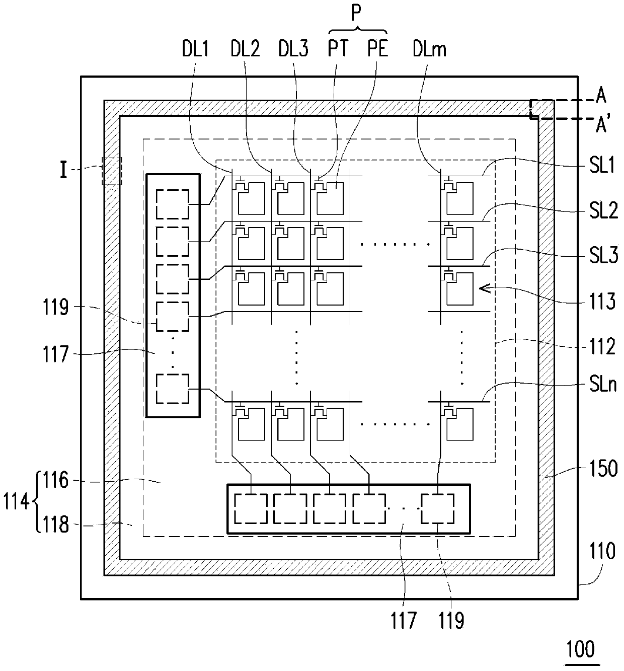
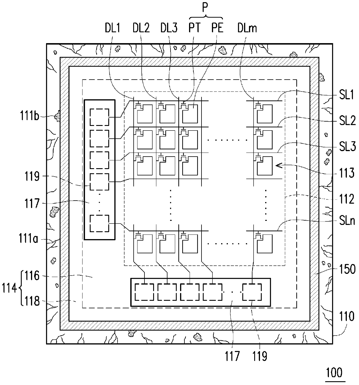
[0100] Figure 8 is a cross-sectional view of a part of the outer area of ​​the display panel according to the first embodiment of the present invention, wherein Figure 8 along figure 2 The cross-sectional view taken by the line A-A'. Please also refer to figure 2 and Figure 8 The outer area 118 of the display panel 100 may include the substrate 110 , the buffer layer 120 , the semiconductor layer 130 , the insulating layer 140 and the metal wall 150 . The material of the substrate 110 can be organic polymer, glass, quartz, or opaque / reflective material (for example: conductive material, metal, wafer, ceramic, or other applicable materials), or other applicable materials .

[0101] The buffer layer 120 can be disposed on the substrate 110 and can be an inorganic thin film made of inorganic materials. For example, the buffer layer 120 can be an inorganic film made of silicon oxide and silicon nitride, and its thickness can be about 350 nanometers (nm), wherein the thi...

no. 2 example

[0107] Figure 9 is a cross-sectional view of a part of the outer area of ​​the display panel according to the second embodiment of the present invention. Please also refer to Figure 8 and Figure 9 The structure of the display panel 200 of the second embodiment is similar to that of the first embodiment, but the difference between them is that the metal wall 250 in the display panel 200 is directly disposed on the buffer layer 120 . In other words, in the outer area of ​​the display panel 200, the buffer layer 120 can be directly disposed on the substrate 110 as an insulating layer without additionally disposing a semiconductor layer and an additional insulating layer, so the metal wall 250 can be directly disposed as an insulating layer. layer on buffer layer 120. It is worth mentioning that since the buffer layer 120 can generally be an inorganic thin film made of inorganic materials and has electrical insulation properties, when the metal wall 250 is directly disposed ...

no. 3 example

[0109] Figure 10 is a cross-sectional view of a part of the outer area of ​​the display panel according to the third embodiment of the present invention. Please also refer to Figure 8 and Figure 10 The structure of the display panel 300 of the third embodiment is mostly the same as that of the first embodiment, but the difference between the two is that the metal wall 350 of the display panel 300 is a multi-layer metal stack structure.

[0110] Please refer to Figure 10 For example, the metal wall 350 can be a metal stack structure composed of a metal layer 350a, a metal layer 350b and a metal layer 350c, wherein the metal layer 350a / metal layer 350b / metal layer 350c can be, for example, Ti / Al / Ti or Mo / Al / Mo multilayer metal stack structure. It is worth mentioning that, as long as the average Poisson's ratio of all metal layers in the metal wall 350 is greater than 0.32, the metal wall 350 may also include a metal layer (such as Mo) whose Poisson's ratio is less than ...


PUM

PropertyMeasurementUnit
thicknessaaaaaaaaaa
thicknessaaaaaaaaaa
thicknessaaaaaaaaaa

Abstract

The invention provides a display panel and a mother board thereof. The display panel comprises a substrate, a pixel array, at least a driving circuit, insulating layers and metal walls, the substrate comprises a display area and a non-display area, the non-display area comprises a driving circuit area and an outside area positioned at the outside of the driving circuit area, the pixel array and the driving circuit are respectively positioned in the display area and the driving circuit area, the insulating layers configured on the substrate and positioned in the non-display area, the metal walls are positioned on the insulating layer and positioned in the outside area, and the Poisson of the metal walls is larger than or equal to 0.32.

Description

technical field [0001] The present invention relates to a display panel and its motherboard, and in particular to a highly reliable display panel and its motherboard. Background technique [0002] With the evolution of optoelectronic and semiconductor technologies, the vigorous development of display panels has been driven. Among many displays, flat panel displays have been widely used recently, and have replaced cathode ray tube displays as the mainstream of next-generation displays. Taking liquid crystal display as an example, display panels usually use inorganic thin films to make active and passive components. The inorganic thin films are usually composed of non-ductile brittle materials such as amorphous silicon, polysilicon, silicon oxide and / or silicon nitride. Therefore, when the display panel is subjected to tensile stress, cracks or peeling are likely to occur in the inorganic thin film, causing damage to active components and / or passive components, thereby affect...

Claims


Application Information

Patent Timeline
Patent Type & Authority Applications(China)
IPC IPC(8): G02F1/133
CPCG02F1/1362G02F1/1333H10K59/12H10K71/851
Inventor 黄震铄杜佳勋王铮亮洪仕馨李孟庭
Owner AU OPTRONICS CORP
Why Eureka
Try Eureka