Semiconductor integrated device

A technology for integrating devices and semiconductors, which is applied in semiconductor devices, electrical solid devices, electrical components, etc., and can solve problems such as damage

Active Publication Date: 2020-12-01
UNITED MICROELECTRONICS CORP
View PDF3 Cites 0 Cited by
  • Summary
  • Abstract
  • Description
  • Claims
  • Application Information

AI Technical Summary

Problems solved by technology

For example, the fin structure of the FinFET device is very susceptible to physical or electrical external forces due to its slender outline, or even be damaged by the above external forces

Method used


Image

  • Semiconductor integrated device
  • Semiconductor integrated device
  • Semiconductor integrated device

Examples


Embodiment Construction

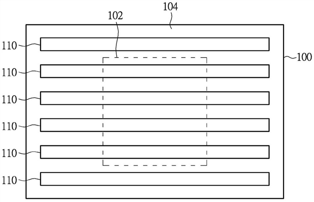
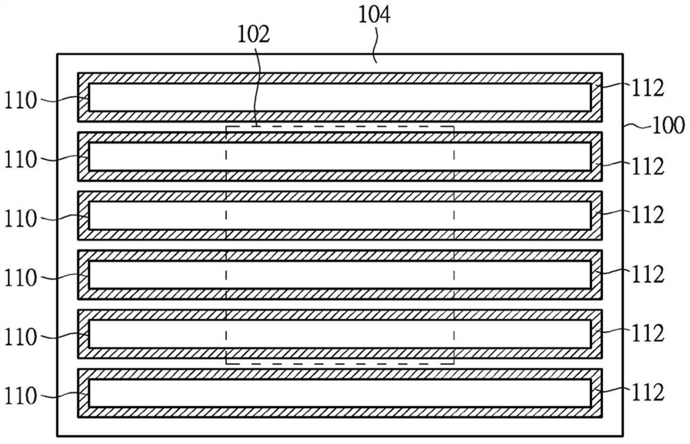
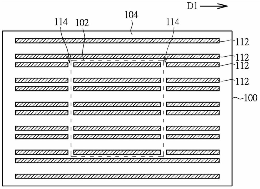
[0034] see Figure 1 to Figure 4 , Figure 1 to Figure 4 It is a schematic diagram of a first preferred embodiment of a semiconductor integrated device provided by the present invention. Such as figure 1 As shown, this preferred embodiment first provides a substrate 100, the substrate 100 may include a silicon-on-insulator (SOI) substrate, as known to those skilled in the art, the SOI substrate can be formed from bottom to top It sequentially includes a silicon substrate, a bottom oxide (BOX) layer, and a semiconductor layer formed on the bottom oxide layer, such as a silicon layer with a single crystal structure. In addition, the substrate provided in this preferred embodiment may include a bulk silicon substrate. An active area 102 and a peripheral area 104 surrounding the active area 102 are defined on the substrate 100 . Those skilled in the art should know that although the peripheral area 104 surrounds the active area 102 in this preferred embodiment, the relative rel...


PUM


Abstract

The invention discloses a semiconductor integrating device which comprises a substrate, a plurality of active fins and a plurality of first protection fins. An active area is at least defined on the substrate, the active fins are arranged in the active area, the first protection fins surround the active area, and the active fins and the first protection fins extend in a first direction.

Description

technical field [0001] The present invention relates to a semiconductor integrated device, in particular to a semiconductor integrated device including a Fin Field effect transistor (FinField effect transistor, hereinafter referred to as FinFET) element and a protection structure. Background technique [0002] When the device is developed to the 65nm technology generation, it is difficult to continue to shrink using the traditional planar metal-oxide-semiconductor (MOS) transistor manufacturing process. Therefore, the existing technology proposes to use three-dimensional or non-planar ) multi-gate transistor components such as FinFET components to replace planar transistor components solution. [0003] Existing FinFET elements first use etching to pattern the silicon layer on the surface of a substrate to form a fin-shaped silicon film (not shown) in the substrate, and form an insulating layer covering part of the silicon film on the silicon film , and then form the gate co...

Claims


Application Information

Patent Timeline
Patent Type & Authority Patents(China)
IPC IPC(8): H01L27/02H01L29/06
Inventor 洪世芳曹博昭
Owner UNITED MICROELECTRONICS CORP
Why Eureka
Try Eureka