A method for preparing a two-dimensional atomic crystal stack structure by transfer

A two-dimensional atomic crystal and stacked structure technology, which is applied in semiconductor/solid-state device manufacturing, electrical components, circuits, etc., can solve the problems of air bubbles, fragile samples, small sample area, etc., to reduce doping and damage, Residual glue treatment is easy and the effect of high separation repetition rate

Active Publication Date: 2020-03-31
SUN YAT SEN UNIV
View PDF4 Cites 0 Cited by
  • Summary
  • Abstract
  • Description
  • Claims
  • Application Information

AI Technical Summary

Problems solved by technology

In this method, the advantage of using mechanical exfoliation to prepare two-dimensional atomic crystal stack structures is that there is less glue residue, and the residual glue treatment is relatively easy, but the disadvantage is that it is very difficult to prepare a single-layer two-dimensional atomic crystal sample, and the peeling The sample is easily broken, the sample area is small, and the technical proficiency is high, and the success rate of preparing the laminated structure sample is low, the repetition rate is low, and the preparation process takes a long time, which is not conducive to practical application
This method uses PMMA to transfer two-dimensional atomic crystals and needs to etch the substrate. The disadvantage of this method is that it takes a long time to etch the substrate, bubbles will be generated during the etching process, and the corrosion ions dope the single-layer atomic crystal material, even Will destroy the structure and reduce the performance of the material itself
In addition, it is difficult to remove clean PMMA glue with acetone, and many organic particles will remain, which will affect the characteristics of the device; in addition, the method of micro-area operation of the probe is used for sample positioning, and the stacking control is poor, and it is difficult to accurately align the sample to prepare ultra-thin Two-dimensional atomic crystal stack structure

Method used


Image

  • A method for preparing a two-dimensional atomic crystal stack structure by transfer
  • A method for preparing a two-dimensional atomic crystal stack structure by transfer
  • A method for preparing a two-dimensional atomic crystal stack structure by transfer

Examples


Embodiment 1

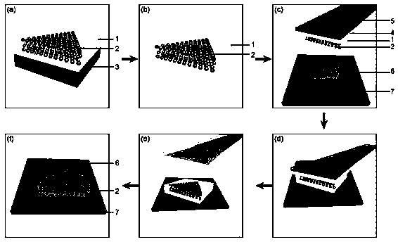
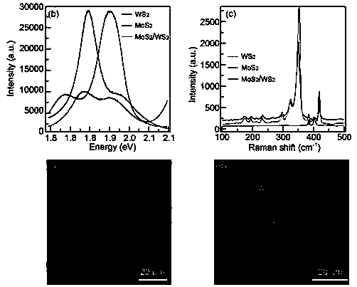
[0038] Positional transfer technology is suitable for the preparation of stacked structures (homojunction and heterojunction) of CVD-grown two-dimensional nanomaterials, so that tungsten disulfide (WS) grown on sapphire substrates 2 / Sapphire) localized molybdenum disulfide (MoS2) transferred to a silicon dioxide substrate 2 / SiO 2 ), so as to prepare a two-dimensional atomic crystal heterojunction as an example, which specifically includes the following steps:

[0039] (1) Toluene was used as a solvent to prepare a polystyrene (PS) solution, and the PS was dissolved by heating with magnetic stirring.

[0040] (2) Prepare dimethylsiloxane (PDMS), mix the main agent (A glue) and the hardener (B glue), remove the air bubbles in the mixed glue by centrifugation, pour it into the container, control the thickness to about 1 mm, and bake curing;

[0041] (3) subbed, in WS 2 / Sapphire surface is spin-coated with PS solution and heated for 30 minutes, then dried toluene solvent; ...

Embodiment 2

[0049] The experimental method is the same as in Example 1, and the single-layer MoS 2 Replaced by single-layer WS 2 , two layers of WS prepared by positioning transfer 2 homogeneous junction.

Embodiment 3

[0051] The experimental method is the same as in Example 1, the only difference is that the monolayer molybdenum disulfide is replaced by molybdenum trioxide nanosheets, and the WS prepared by positioning transfer 2 / MoO 3 Heterojunction.


PUM

PropertyMeasurementUnit
thicknessaaaaaaaaaa

Abstract

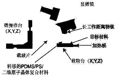
The invention discloses a method for transferring and preparing a two-dimensional atomic crystal laminated structure and relates to a stripping, positioning and transferring method for substrate-based two-dimensional atomic crystal film. The method comprises the specific steps of carrying out spin-coating on the surface of the two-dimensional atomic crystal film through utilization of polystyrene film, wherein the two-dimensional atomic crystal film is prepared based on a substrate; separating two-dimensional atomic crystals from the substrate through utilization of water tension and transferring the two-dimensional atomic crystals to dimethyl siloxane polymer; attaching the two-dimensional atomic crystals / polystyrene / dimethyl siloxane polymer on a target material through utilization of the van-der waals force; and separating the dimethyl siloxane polymer in a heating mode and removing the polystyrene through utilization of toluene solution or a vacuum annealing method, namely preparing the two-dimensional atomic crystal laminated structure. The method is simple in operation and is high in success rate, is fast and can be widely applied to the field of a large-area ultra-thin material photoelectric sensor.

Description

technical field [0001] The invention relates to the technical field of positioning transfer, and more specifically, to a method for preparing a two-dimensional atomic crystal stack structure by transfer. Background technique [0002] New two-dimensional atomic crystals include graphene, boron nitride, black phosphorus and two-dimensional transition metal chalcogenides, such as: molybdenum disulfide, molybdenum diselenide, molybdenum ditelluride, tungsten disulfide, tungsten diselenide and Tungsten ditelluride, etc., which have unique properties of force, heat, electricity, and light, have attracted the attention of researchers. Then people have also carried out a series of studies based on new two-dimensional atomic-level stacked structures, among which the preparation of ultra-thin two-dimensional The stacked structure of atomic crystals has become a research hotspot in the application field of optoelectronic materials and devices, such as high electron mobility tunnel fiel...

Claims


Application Information

Patent Timeline
Patent Type & Authority Patents(China)
IPC IPC(8): H01L21/78H01L21/18
CPCH01L21/187H01L21/7806
Inventor 陈焕君温锦秀邓少芝许宁生
Owner SUN YAT SEN UNIV
Why Eureka
Try Eureka