DMOS device and manufacturing method thereof

A manufacturing method and device technology, which is applied in semiconductor/solid-state device manufacturing, semiconductor devices, electrical components, etc., can solve the problems of chip conduction current difference and low cell integration, and achieve the goal of reducing distance and improving integration Effect

Active Publication Date: 2014-12-24
FOUNDER MICROELECTRONICS INT
View PDF5 Cites 3 Cited by
  • Summary
  • Abstract
  • Description
  • Claims
  • Application Information

AI Technical Summary

Problems solved by technology

Therefore, the photolithography process to make the source region limits the distance between the cell trenches, resulting in low integration of the cells in the DMOS device, and poor conduction current per unit area of ​​the chip.

Method used


Image

  • DMOS device and manufacturing method thereof
  • DMOS device and manufacturing method thereof
  • DMOS device and manufacturing method thereof

Examples


Embodiment Construction

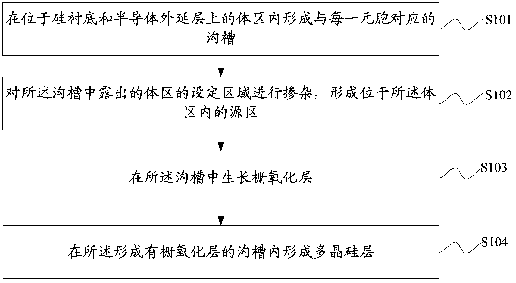
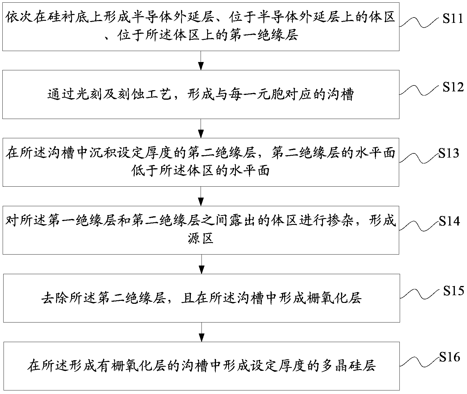
[0058] Embodiments of the present invention provide a DMOS device and a manufacturing method thereof, which are used to reduce the distance between adjacent cells on the DMOS device and improve the integration degree of the DMOS device.

[0059] The technical solutions provided by the embodiments of the present invention can be applied to the manufacture of trench-type DMOS devices.

[0060] In the method for fabricating a DMOS device provided by an embodiment of the present invention, a trench is first formed on the body region to expose the body region in the trench, and a set region in the exposed body region is doped to form a source region in the trench . The registration deviation caused by the existing photolithography process to form the source area is avoided, the distance between adjacent cells is reduced, and the integration degree of the DMOS device is improved.

[0061] The DMOS device provided by the embodiment of the present invention may include an N-type or P...


PUM


Abstract

The invention discloses a DMOS device and a manufacturing method of the DMOS device. The DMOS device and the manufacturing method of the DMOS device are used for increasing the density of cells of the DMOS device. The method comprises the first step of forming grooves corresponding to the cells in a body area located on a silicon substrate and a semiconductor epitaxial layer, the second step of conducting doping on set areas of the body area exposed out of the grooves to form source areas located in the body area, the third step of growing a gate oxidation layer in the grooves, and the fourth step of forming a polycrystalline silicon layer in the grooves where the gate oxidation layer is formed.

Description

technical field [0001] The invention relates to the technical field of semiconductor chip manufacturing technology, in particular to a double-diffused metal oxide semiconductor (Double-diffused Metal Oxide Semiconductor, DMOS) device and a manufacturing method thereof. Background technique [0002] With the development of electronic technology, the design of electronic products has higher and higher requirements for components. At present, under the requirement of maximizing the chip integration density, the size of the chip is also continuously reduced in proportion. Correspondingly, more and more challenges are encountered in the process of manufacturing trench DMOS devices. A DMOS device is composed of many cells side by side. To make a DMOS device with a higher integration level on a wafer, that is, to make a larger number of cells on a wafer, it is necessary to ensure the performance of the device. The distance between cells can be reduced as soon as possible. For tren...

Claims


Application Information

Patent Timeline
Patent Type & Authority Applications(China)
IPC IPC(8): H01L29/78H01L29/06H01L21/336
CPCH01L29/66689H01L29/66704H01L29/7825
Inventor 马万里
Owner FOUNDER MICROELECTRONICS INT
Why Eureka
Try Eureka