

A method of improving exposure precision of hdi circuit board
A technology of exposure accuracy and circuit board, applied in the direction of printed circuit, printed circuit manufacturing, electrical components, etc., can solve the problems of line deformation, affecting the performance of circuit board products, damage to adjacent layers of products
- Summary
- Abstract
- Description
- Claims
- Application Information
AI Technical Summary
Problems solved by technology
Method used
Image

Examples
Embodiment 1
[0023] A method for improving the exposure accuracy of HDI circuit boards, comprising the following steps:
[0024] a. Drill 4 through-hole alignment holes through mechanical drilling on the non-line area of the four top corners of the copper clad laminate;
[0025] b. On the periphery of each through-hole alignment hole on the copper-clad laminate, remove the copper layer, and drill a blind hole alignment hole group at the position without the copper layer through laser drilling; the blind hole alignment hole group includes 8 Blind hole alignment holes surrounding the periphery of the through hole alignment holes;
[0026] c. In the exposure process, the film used is provided with through-hole targets and blind-hole targets corresponding to the through-hole alignment holes and blind hole alignment holes; before exposure, the through-hole alignment holes and through-hole targets are first Carry out pre-alignment so that the through-hole target and the corresponding through-...
Embodiment 2
[0033] A method for improving the exposure accuracy of HDI circuit boards, comprising the following steps:
[0034] a. Drill 4 through-hole alignment holes through mechanical drilling on the non-line area of the four top corners of the copper clad laminate;
[0035] b. On the periphery of each through-hole alignment hole on the copper-clad board, remove the copper layer, and drill a blind hole alignment hole group at the position without the copper layer through laser drilling; the blind hole alignment hole group includes 8 Blind hole alignment holes surrounding the periphery of the through hole alignment holes;
[0036] c. In the exposure process, the film used is provided with through-hole targets and blind-hole targets corresponding to the through-hole alignment holes and blind hole alignment holes; before exposure, first pass through the through-hole alignment holes and through-hole targets Carry out pre-alignment so that the through-hole target and the corresponding th...
Embodiment 3
[0043] A method for improving the exposure accuracy of HDI circuit boards, comprising the following steps:
[0044] a. Drill 4 through-hole alignment holes through mechanical drilling on the non-line area of the four top corners of the copper clad laminate;
[0045] b. On the periphery of each through-hole alignment hole on the copper-clad board, remove the copper layer, and drill a blind hole alignment hole group at the position without the copper layer through laser drilling; the blind hole alignment hole group includes 8 Blind hole alignment holes surrounding the periphery of the through hole alignment holes;
[0046] c. In the exposure process, the film used is provided with through-hole targets and blind-hole targets corresponding to the through-hole alignment holes and blind hole alignment holes; before exposure, first pass through the through-hole alignment holes and through-hole targets Carry out pre-alignment so that the through-hole target and the corresponding th...
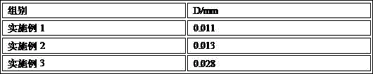
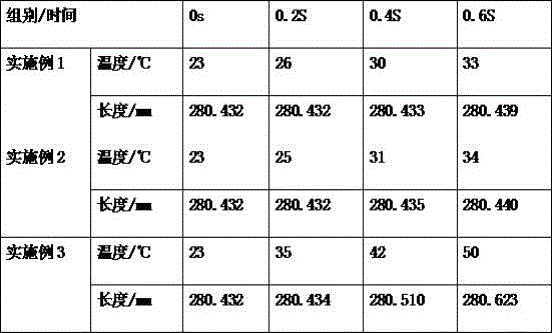
PUM
 Abstract
Description
Claims
Application Information