Fin field effect transistor and forming method thereof

A fin field effect and transistor technology, which is applied in the fields of semiconductor devices, semiconductor/solid-state device manufacturing, electrical components, etc., can solve problems such as difficulty in adjusting the threshold voltage of fin field effect transistors, and achieve power saving and strong adjustment ability. , the effect of the transmission path is short

Active Publication Date: 2014-12-31
SEMICON MFG INT (SHANGHAI) CORP
View PDF5 Cites 11 Cited by
  • Summary
  • Abstract
  • Description
  • Claims
  • Application Information

AI Technical Summary

Problems solved by technology

[0004] When the existing fin field effect transistors are in use, the bias control voltage is usually connected to the semiconductor substrate 10 to adjust the threshold voltage of the fin field effect transistors, but the existing adjustment methods have no effect on the fin field effect transistors. It is difficult to adjust the threshold voltage of the transistor

Method used


Image

  • Fin field effect transistor and forming method thereof
  • Fin field effect transistor and forming method thereof
  • Fin field effect transistor and forming method thereof

Examples


Embodiment Construction

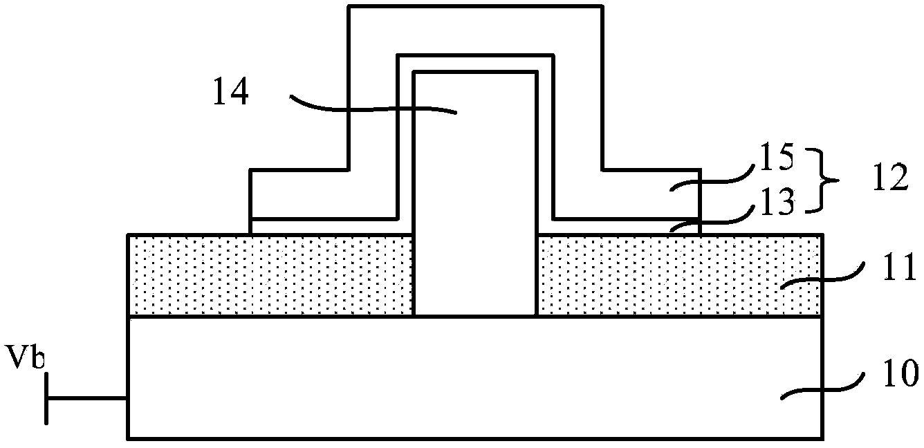
[0034] reference figure 1 In the prior art, when adjusting the threshold voltage of a fin-type field effect transistor, the bias control voltage Vb is usually connected to the semiconductor substrate 10. The inventor found that the bias control voltage Vb needs to pass through the semiconductor substrate 10 and the fin. 14 can be conducted to the vicinity of the surface of the fin 14 at the bottom of the gate structure 12, so that the conduction path of the bias control voltage Vb is very long, and the resistance on the conduction path is relatively large. Therefore, the bias control voltage Vb is applied to the gate structure 12 The electric potential on the surface of the bottom fin 14 is very small, which is not conducive to adjusting the threshold voltage of the fin field effect transistor, and the bias control voltage Vb has a weak ability to adjust the threshold voltage. In order to enhance the ability of the bias control voltage Vb to adjust the threshold voltage, one app...


PUM


Abstract

The invention discloses a fin field effect transistor and a forming method thereof. The fin field effect transistor comprises a semiconductor substrate, a first doping layer, an isolating layer, a gate structure, a dielectric layer, a through hole and a conductive plug, wherein first fin parts and a second fin part which are discrete are formed on the semiconductor substrate; the first doping layer covers the first fin parts, the second fin part and the surface of the semiconductor substrate; the isolating layer is located on the semiconductor substrate; the surface of the isolating layer is lower than the surface of the first doping layer at the top ends of the first fin parts and the second fin part; the gate structure crosses side wall and top end surfaces of the first fin parts; the dielectric layer is located on the isolating layer, and covers the gate structure and the second fin part; the through hole is located in the dielectric layer, and exposed out of the first doping layer at the top end of the second fin part; and the conductive plug fills the through hole, and is connected with bias control voltage. Regulation of threshold voltage can be conveniently achieved by the conductive plug and the first doping layer.

Description

Technical field [0001] The invention relates to the field of semiconductor manufacturing, in particular to a fin field effect transistor and a method for forming the same. Background technique [0002] With the continuous development of semiconductor process technology, process nodes are gradually reduced, and the gate-last process has been widely used to obtain ideal threshold voltage and improve device performance. However, when the feature size (CD, Critical Dimension) of the device is further reduced, even if the gate-last process is adopted, the structure of the conventional MOS field effect transistor can no longer meet the requirements for device performance, and the fin field effect transistor (Fin FET) is used as The replacement of conventional devices has received extensive attention. [0003] figure 1 The structure diagram of a fin field effect transistor in the prior art is shown. Such as figure 1 As shown, it includes: a semiconductor substrate 10 on which a protrudi...

Claims


Application Information

Patent Timeline
Patent Type & Authority Applications(China)
IPC IPC(8): H01L21/336H01L21/28H01L29/78H01L29/423
CPCH01L21/823431H01L21/845H01L29/6681H01L29/785
Inventor 三重野文健
Owner SEMICON MFG INT (SHANGHAI) CORP
Why Eureka
Try Eureka