Method for forming CMOS (Complementary Metal-Oxide-Semiconductor) transistor

A transistor and gas technology, applied in the field of formation of CMOS transistors, can solve the problems of complex process steps and poor performance of CMOS transistors, and achieve the effects of simple process, reduction of formation time, and reduction of adverse effects

Active Publication Date: 2014-12-31
SEMICON MFG INT (SHANGHAI) CORP
View PDF6 Cites 5 Cited by
  • Summary
  • Abstract
  • Description
  • Claims
  • Application Information

AI Technical Summary

Problems solved by technology

[0005] However, the CMOS transistors formed by the prior art have poor performance and complicated process steps

Method used


Image

  • Method for forming CMOS (Complementary Metal-Oxide-Semiconductor) transistor
  • Method for forming CMOS (Complementary Metal-Oxide-Semiconductor) transistor
  • Method for forming CMOS (Complementary Metal-Oxide-Semiconductor) transistor

Examples


Embodiment Construction

[0032] It can be seen from the background art that the performance of forming CMOS transistors in the prior art is poor and the process steps are complicated.

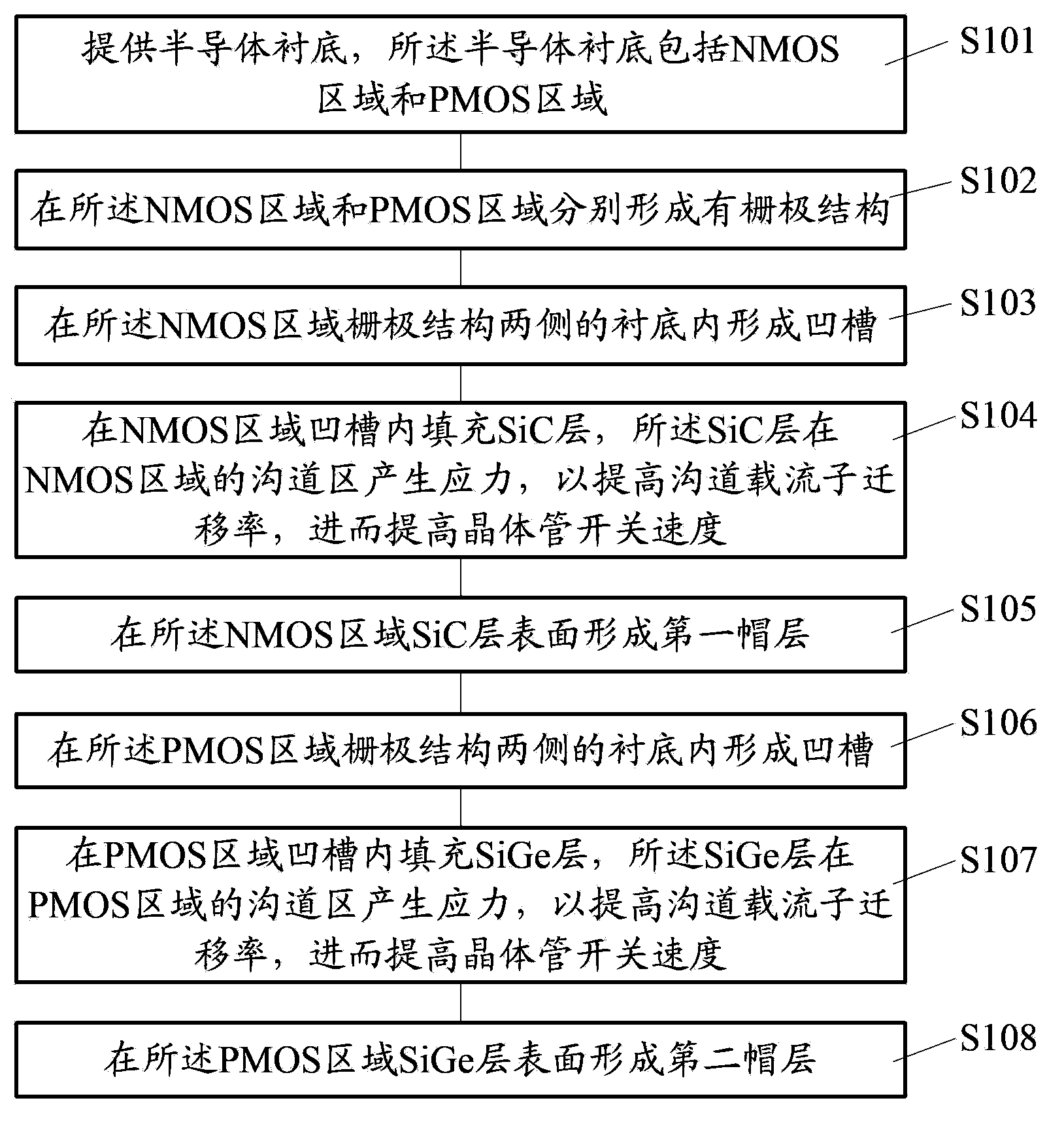
[0033] For this reason, the inventor studies the prior art CMOS transistor formation process, and finds that the CMOS transistor formation process includes the following steps, please refer to figure 1 Step S101, providing a semiconductor substrate, the semiconductor substrate includes an NMOS region and a PMOS region; Step S102, forming a gate structure in the NMOS region and the PMOS region respectively; Step S103, forming a gate structure in the NMOS region Grooves are formed in the substrates on both sides; step S104, filling the SiC layer in the groove of the NMOS region, and the SiC layer generates stress in the channel region of the NMOS region to increase the carrier mobility of the channel, thereby improving the transistor Switching speed; step S105, forming a first cap layer on the surface of the SiC layer in...


PUM


Abstract

The invention discloses a method for forming a CMOS (Complementary Metal-Oxide-Semiconductor) transistor. The method comprises the following steps: providing a semiconductor substrate; forming gate structures on the first region and the second region of the semiconductor substrate; forming first grooves in the semiconductor substrate on both sides of the gate structure in the first region; filling the first grooves with first stress layers; forming second grooves in the semiconductor substrate on both sides of the gate structure in the second region; filling the second grooves with second stress layers, wherein the stress types of the second stress layers are opposite to those of the first stress layers; and forming first cap layers on the surfaces of the first stress layers, and meanwhile forming second cap layers on the surfaces of the second stress layers. Through adoption of the forming method disclosed by the invention, thermal budget in the forming process of the CMOS transistor is reduced, and the reliability and electrical performance of the CMOS transistor are enhanced.

Description

technical field [0001] The invention relates to the field of semiconductor manufacturing, in particular to a method for forming a CMOS transistor. Background technique [0002] Complementary Metal-Oxide-Semiconductor (CMOS) transistors have become commonly used semiconductor devices in integrated circuits. The CMOS transistors include: P-type metal oxide semiconductor (PMOS) transistors and N-type metal oxide semiconductor (NMOS) transistors. [0003] As element density and integration of semiconductor devices increase, the gate size of PMOS transistors or NMOS transistors becomes shorter than before. However, the shortening of the gate size of the PMOS transistor or the NMOS transistor will produce a short channel effect, thereby generating a leakage current and affecting the electrical performance of the CMOS transistor. In the prior art, the carrier mobility is mainly increased by increasing the stress of the channel region of the transistor, thereby increasing the driv...

Claims


Application Information

Patent Timeline
Patent Type & Authority Applications(China)
IPC IPC(8): H01L21/8238
CPCH01L21/8238
Inventor 涂火金
Owner SEMICON MFG INT (SHANGHAI) CORP
Why Eureka
Try Eureka