Organic electroluminescent device, manufacturing method thereof and display device

An electroluminescent device and electroluminescent layer technology, which is applied in the manufacturing of organic semiconductor devices, electric solid state devices, semiconductor/solid state devices, etc. The effect of improving yield, improving quality and reducing poor contact

Active Publication Date: 2015-01-07
BOE TECH GRP CO LTD
View PDF7 Cites 21 Cited by
  • Summary
  • Abstract
  • Description
  • Claims
  • Application Information

AI Technical Summary

Problems solved by technology

[0005] For the upper auxiliary electrode scheme, the color filter substrate and the OLED substrate are pressed together under vacuum, and the conductive layer on the spacer is in contact with the cathode under pressure and deforms. There are two problems: 1. Spacer deformation It may cause the conductive layer to break, and there is a danger of disconnection of the auxiliary electrode and the cathode connection, so the pressing force must be precisely controlled; 2. Since the conductive layer and the cathode contact on the spacer are in surface contact, there is a risk of poor contact
[0006] For the lower auxiliary electrode scheme, in order to solv

Method used


Image

  • Organic electroluminescent device, manufacturing method thereof and display device
  • Organic electroluminescent device, manufacturing method thereof and display device
  • Organic electroluminescent device, manufacturing method thereof and display device

Examples


no. 1 example

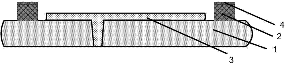
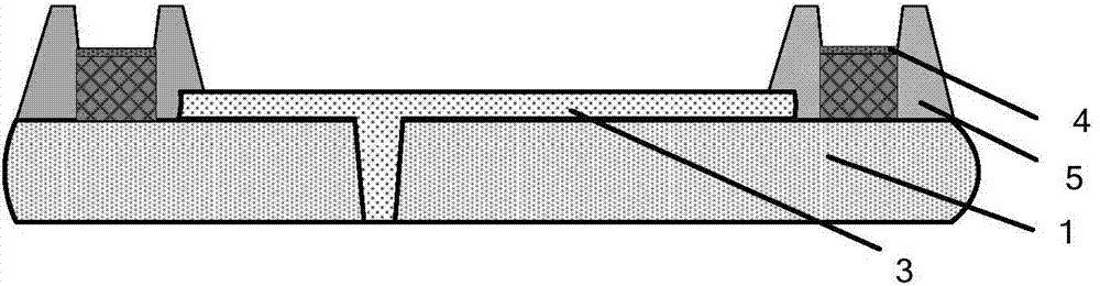
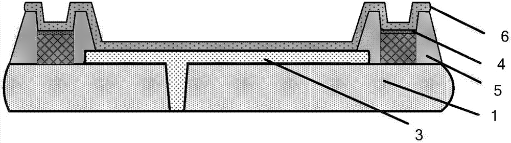
[0036] Such as Figure 1~6 As shown, according to the first embodiment of the present invention, a method for preparing an organic electroluminescent device is provided, comprising the following steps:

[0037] S1, forming an auxiliary electrode on the resin resin layer of the organic electroluminescent substrate;

[0038] S2. Forming a gas generation layer on the auxiliary electrode;

[0039] S3, forming an organic electroluminescent layer on the gas generating layer;

[0040] S4. Place a receptor substrate on the organic electroluminescent layer, and then scan the auxiliary electrode region with a laser, so that the gas generating layer decomposes under laser irradiation and releases gas, so that the active part of the auxiliary electrode region is transferring an electroluminescent layer onto said receptor substrate;

[0041] S5. Removing the acceptor substrate;

[0042] S6, forming a cathode on the auxiliary electrode.

[0043] Among them, the auxiliary electrode is p...


PUM

PropertyMeasurementUnit
Thicknessaaaaaaaaaa
Thicknessaaaaaaaaaa

Abstract

The invention discloses a manufacturing method of an organic electroluminescent device. The method includes the steps that an auxiliary electrode is formed on a resin layer of an organic electroluminescent substrate; a gas generation layer is formed on the auxiliary electrode; an organic electroluminescent layer is formed on the gas generation layer; an accepter substrate is arranged on the organic electroluminescent layer; an auxiliary electrode area is scanned through laser, so that the gas generation layer is decomposed under laser radiation and releases gas, and accordingly the organic electroluminescent layer of the auxiliary electrode area is transferred to the accepter substrate; the accepter substrate is removed; a cathode is formed on the auxiliary electrode. By means of the new top-emitting OLED device auxiliary electrode manufacturing technology, bad contact between the auxiliary electrode and the cathode can be effectively reduced, the pixel defect caused due to the fact that residues generated after an organic material or the cathode is sintered and melted through laser are transferred to a pixel area in following processes is avoided, quality of the electroluminescent device is improved, and the yield is improved.

Description

technical field [0001] The invention belongs to the field of display technology, and in particular relates to an organic electroluminescence device, a preparation method thereof, and a display device. Background technique [0002] Compared with LCD (Liquid Crystal Display), organic electroluminescent devices (Organic Light-Emitting Diode, OLED) have the advantages of self-luminescence, fast response, wide viewing angle, high brightness, bright colors, light and thin, etc., and are considered to be the next generation display. technology. Existing OLED devices are usually composed of an anode layer, a light-emitting layer and a cathode layer. According to the different light-emitting surfaces, they can be divided into two types: bottom emission and top emission. Because top emission devices can obtain a larger aperture ratio, they have become a research hotspot in recent years. Top-emitting OLEDs require thin cathodes and reflective anodes to increase light transmittance, an...

Claims


Application Information

Patent Timeline
IPC IPC(8): H01L51/50H01L51/56H01L27/32
CPCH10K59/00H10K50/00H10K50/80H10K59/10H10K71/00H10K59/38H10K59/122H10K71/211H10K71/18H10K71/50H10K50/824H10K2102/3026H10K71/811H10K50/818H10K50/828H10K59/1201H10K2102/351
Inventor 王辉锋
Owner BOE TECH GRP CO LTD
Why Eureka
Try Eureka