Substrate with interference type optical filter layer and displaying device with substrate

A technology for display devices and optical filters, applied in the direction of optical filters, optics, optical components, etc., can solve problems such as loss and achieve high light utilization efficiency

Inactive Publication Date: 2015-01-14
KK TOSHIBA
View PDF6 Cites 9 Cited by
  • Summary
  • Abstract
  • Description
  • Claims
  • Application Information

AI Technical Summary

Problems solved by technology

Therefore, for example, when the white light entering the liquid crystal display device from the backlight installed on the back of the liquid crystal display device passes through the blue filter, the green and red light are absorbed by the blue filter. Therefore, will cause loss

Method used


Image

  • Substrate with interference type optical filter layer and displaying device with substrate
  • Substrate with interference type optical filter layer and displaying device with substrate
  • Substrate with interference type optical filter layer and displaying device with substrate

Examples


Embodiment 1

[0071] FIG. 7 shows a method of manufacturing a substrate with an interference filter layer according to the first embodiment.

[0072] As shown in FIG. 7( a ), a silicon oxide film of 100 nm was formed on a glass substrate 1 by CVD as an undercoat layer 7 . Next, 25 nm of Ag was deposited on the entire surface by vacuum evaporation to form the first reflective layer 2 . Next, a silicon oxide film was formed with a thickness of 100 nm by CVD to form the first spacer layer 4 , and a silicon nitride film was formed with a thickness of 25 nm by CVD to form the second spacer layer 5 . Next, the photosensitive resist layer 23 is patterned on the second spacer layer 5 , and the second spacer layer 5 is etched by chemical dry etching to remove the resist layer 23 .

[0073] When performing etching, the etching conditions of chemical dry etching are as follows: if the selectivity ratio of the silicon nitride film and the silicon oxide film is high enough, that is, the etching speed o...

Embodiment 2

[0084] The difference between Embodiment 2 and Embodiment 1 lies in that the patterns of the first space, the second space, and the third space constituting the optical filter layer are different. The same reference numerals are assigned to the same structures as those in Embodiment 1, and descriptions of the same structures are omitted.

[0085] FIG. 9 shows another example of the substrate with a filter layer and its manufacturing method related to the second embodiment.

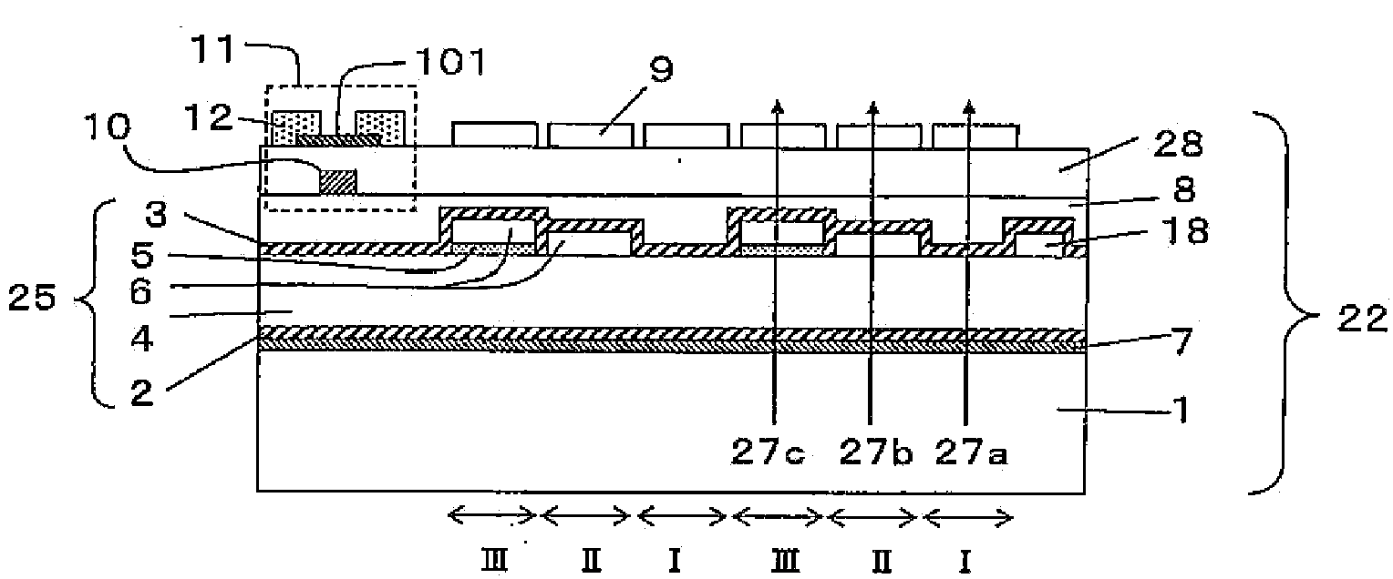
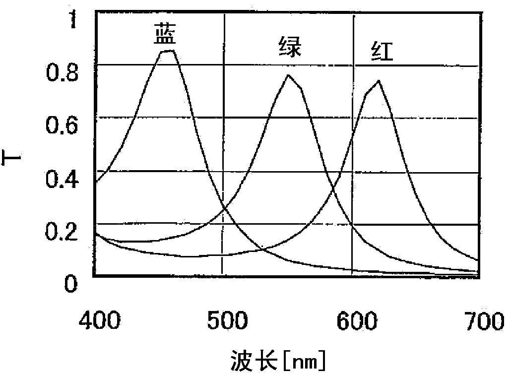
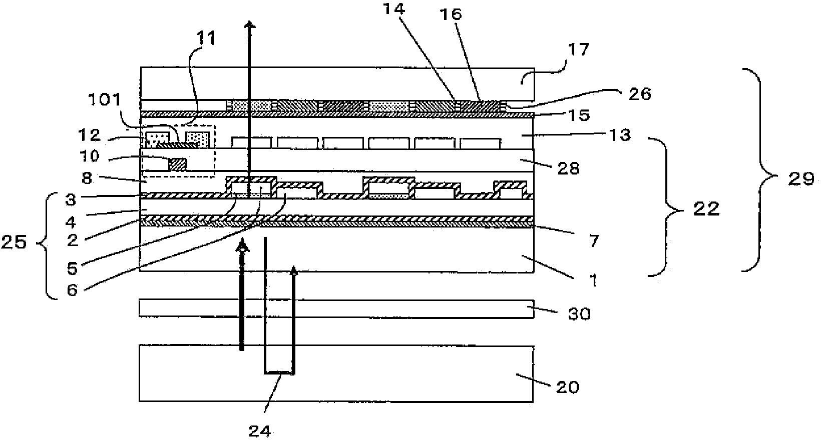
[0086] The manufactured substrate with a filter layer of Example 2 is shown in FIG. 9( c ), and the structure of the filter layer 25 is different from that of Example 1. That is, in the filter layer 25 of Example 2, the second spacer layer 5 is provided on a part of the first spacer layer 4 . In addition, the third spacer layer 6 is provided on a part of the region where the second spacer layer 5 is not provided on the first spacer layer 4 . Therefore, the filter layer 25 has three types: a region I havi...

Embodiment 3

[0093] In addition, it is also possible to use Figure 10 that kind of structure. That is, the second spacer layer 5 is provided at least two places on the first reflective layer 2 . The first spacer layer 4 is disposed on the second spacer layer 5 and the first reflective layer 2 . Furthermore, a third spacer layer 6 is provided on the first spacer layer 4 provided on one of the two second spacer layers 5 .

[0094] In addition, the third spacer layer 6 is also provided on a portion of the first spacer layer 4 where the second spacer layer 5 is not provided.

[0095] Thus, the filter layer 25 has the following four regions. That is, the filter layer 25 has a region I in which only the first spacer layer 4 is used as a transmissive layer, a region II in which the first spacer layer 4 is provided on the second spacer layer 5, and a region II in which the first spacer layer 4 is provided on the first spacer layer 4. Region III with three spacer layers 6 and region IV with se...


PUM

PropertyMeasurementUnit
thicknessaaaaaaaaaa
thicknessaaaaaaaaaa
thicknessaaaaaaaaaa

Abstract

The invention discloses a substrate with an interference type optical filter layer and a displaying device with the substrate. The substrate can be formed by a small number of processes, and light using efficiency is high. The substrate with the interference type optical filter layer comprises a flat plate type substrate and the optical filter layer which comprises a first reflecting layer, a transmission layer and a second reflecting layer. The first reflecting layer is arranged on the substrate and has light half-transmission performance. The transmission layer is formed by a first partitioning layer which is arranged on the first reflecting layer and has light transmission performance, a second partitioning layer which is arranged on part of the first reflecting layer and has light transmission performance and a third partitioning layer, and a first zone, a second zone and a third zone are arranged. The first zone, the second zone and the third zone share the first partitioning layer. The optical film thicknesses of the first zone, the second zone and the third zone are different due to the second partitioning layer and the third partitioning layer, the second reflecting layer is arranged on the transmission layer and has light half-transmission performance, and light with different wavelengths is transmitted through the first zone, the second zone and the third zone through the optical filter layer.

Description

[0001] This application is a divisional application of the application date "January 21, 2010", the application number "201080055911.4", and the title "substrate with interference filter layer and display device using the substrate". technical field [0002] The invention relates to a substrate with an interference filter layer and a display device using the substrate. Background technique [0003] With the start of terrestrial digital broadcasting, the spread of the Internet, and mobile phones, the demand for display devices such as liquid crystal displays and plasma displays is increasing. Some of these displays are mounted on mobile devices as small displays, but on the other hand, the demand for large-screen TVs is also expanding. [0004] In conventional displays, matrix wiring is provided on a glass substrate, and especially in the case of a liquid crystal display, thin film transistors are provided at intersections of matrix wiring. The opposing substrate is arranged...

Claims


Application Information

Patent Timeline
Patent Type & Authority Applications(China)
IPC IPC(8): G02B5/28G02B5/20G02F1/1335
CPCG02B5/285G02F1/133514G02F1/133516G02F1/133521
Inventor 中井 豊小野 富男本宫 佳典额田 秀记平山 雄三永户 一志宫崎 崇
Owner KK TOSHIBA
Why Eureka
Try Eureka