Forming method of interconnection structure

A technology of interconnection structure and single-layer structure, which is applied in the manufacturing of electrical components, electric solid-state devices, semiconductor/solid-state devices, etc., can solve the problem of increased RC delay of interconnection structure, reduced reliability of interconnection structure, damage of dielectric layer, etc. problem, to achieve the effect of improving the anti-electromigration characteristics and improving the ability

Active Publication Date: 2015-01-21
SEMICON MFG INT (SHANGHAI) CORP
View PDF8 Cites 3 Cited by
  • Summary
  • Abstract
  • Description
  • Claims
  • Application Information

AI Technical Summary

Problems solved by technology

[0005] However, the process of forming the interconnection structure in the prior art will cause a certain degree of damage to the dielectric layer of the interconnection structure, resulting in an increas...

Method used


Image

  • Forming method of interconnection structure
  • Forming method of interconnection structure
  • Forming method of interconnection structure

Examples


Embodiment Construction

[0034] It can be seen from the background art that the dielectric layer of the interconnection structure formed in the prior art will be affected by the formation process, resulting in an increase in the dielectric constant of the dielectric layer and an increase in the RC delay of the interconnection structure.

[0035] In order to solve the above-mentioned problems, research is being conducted on the formation method of the interconnection structure.

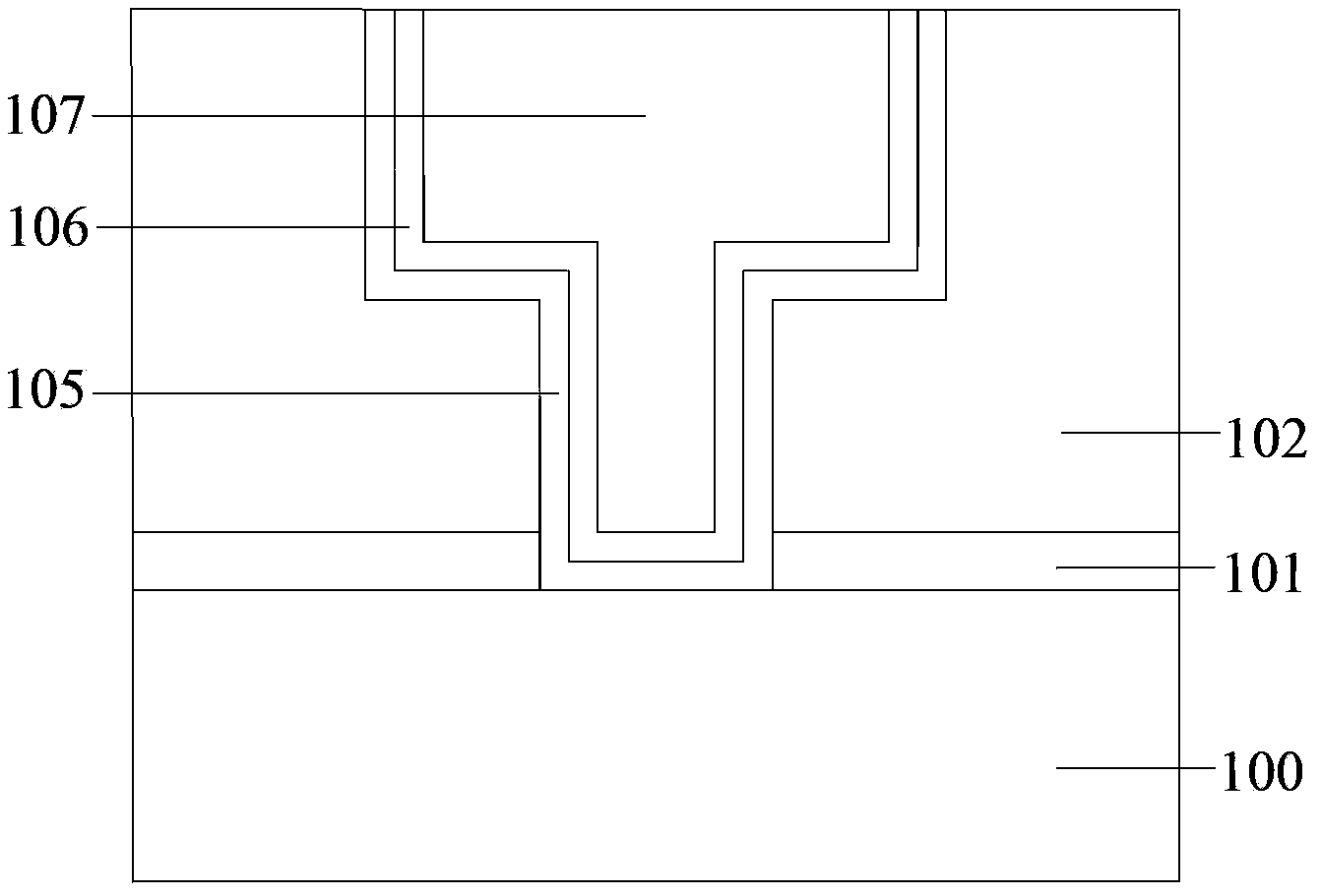
[0036] Please refer to figure 1 , provide a semiconductor substrate 100, the surface of the semiconductor substrate 100 is formed with a dielectric layer, the dielectric layer includes an etching stopper layer 101 on the surface of the semiconductor substrate 100 and a dielectric layer 102 on the surface of the etching stopper layer 101; An opening is formed in the layer, and the bottom of the opening exposes the surface of the semiconductor substrate 100; a metal layer filling the opening is formed in the opening, and the me...


PUM

PropertyMeasurementUnit
Thicknessaaaaaaaaaa

Abstract

The invention discloses a forming method of an interconnection structure. The forming method comprises the following steps: providing a semiconductor substrate, wherein a dielectric layer is formed on the surface of the semiconductor substrate; forming an opening in the dielectric layer, wherein the bottom of the opening is exposed out of the surface of the semiconductor substrate; forming a metal layer filling the opening in the opening, wherein the surface of the metal layer is flush with the top of the dielectric layer; introducing methyl-containing germane gas into the surfaces of the metal layer and the dielectric layer, and performing germanium treatment on the surface of the metal layer to form a metal cap layer; and forming a dielectric cap layer on the surfaces of the metal cap layer and the dielectric layer. Through adoption of the forming method of the interconnection structure disclosed by the invention, damage to the dielectric layer of the interconnection structure can be effectively reduced while the electromigration resistance of the interconnection structure is enhanced; the RC (Resistance-Capacitance) delay of the interconnection structure is reduced; and the reliability of the interconnection structure is enhanced.

Description

technical field [0001] The invention relates to the field of semiconductor manufacturing, in particular to a method for forming an interconnection structure. Background technique [0002] With the development of semiconductor technology, the integration level of VLSI chips has reached hundreds of millions or even billions of devices, and multi-layer metal interconnection technology with more than two layers is widely used. Traditional metal interconnects are made of aluminum metal, but with the continuous reduction of device feature size in integrated circuit chips, the circuit density in metal interconnect lines continues to increase, and the required response time continues to decrease. Traditional aluminum Interconnection wires can no longer meet the requirements, and copper interconnection technology gradually replaces aluminum interconnection technology. Compared with aluminum, copper has lower resistivity and higher anti-electromigration characteristics, which can red...

Claims


Application Information

Patent Timeline
IPC IPC(8): H01L21/768
CPCH01L21/76886H01L2221/1068
Inventor 邓浩
Owner SEMICON MFG INT (SHANGHAI) CORP
Why Eureka
Try Eureka