Method for improving compiling speed of silicon-oxide-nitride-oxide-silicon (SONOS) structure device by using stress technology

A technology of stress and technology, which is applied in the field of using stress technology to improve the compilation speed of SONOS structure devices, can solve the problems such as the effect of stress transfer is not obvious, achieve the effect of improving carrier mobility, the effect is obvious, and the interface state is improved

Active Publication Date: 2015-05-20
SHANGHAI HUALI MICROELECTRONICS CORP
View PDF7 Cites 0 Cited by
  • Summary
  • Abstract
  • Description
  • Claims
  • Application Information

AI Technical Summary

Problems solved by technology

[0007] The purpose of the present invention is to solve the problem that the stress transfer effect of the existing stress memory technology on the SONOS structure device is not obvious, and improve the carrier mobility

Method used


Image

  • Method for improving compiling speed of silicon-oxide-nitride-oxide-silicon (SONOS) structure device by using stress technology
  • Method for improving compiling speed of silicon-oxide-nitride-oxide-silicon (SONOS) structure device by using stress technology
  • Method for improving compiling speed of silicon-oxide-nitride-oxide-silicon (SONOS) structure device by using stress technology

Examples


no. 1 example

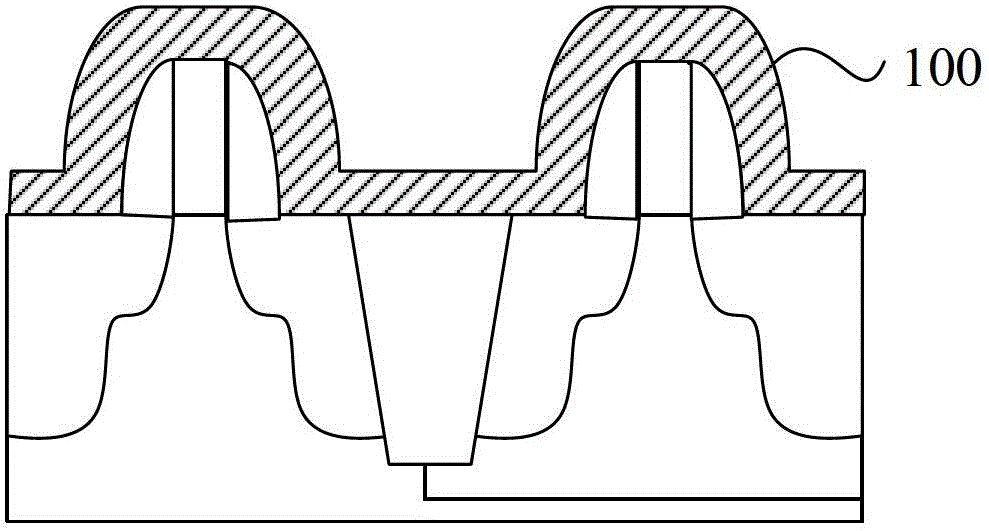
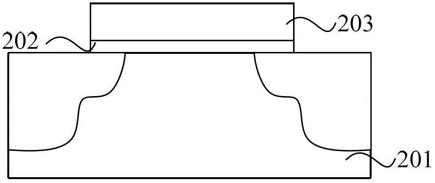
[0046] Please refer to figure 2 and Figure 3a-Figure 3f ,in, figure 2 It is a flowchart of a method for improving the compiling speed of a SONOS structure device using stress technology in the first embodiment of the present invention, Figure 3a-Figure 3f It is a schematic diagram of the process steps of introducing stress in the first embodiment of the present invention.

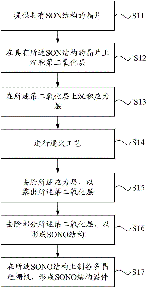
[0047] first reference figure 2 , the method for improving the compiling speed of a SONOS structure device by using the stress technique comprises the following steps:

[0048] Step S11, providing a wafer with a SON structure, the SON structure is a silicon semiconductor substrate, a first oxide layer, and a storage nitride layer in sequence from bottom to top;

[0049] Step S12, depositing a second oxide layer on the wafer having the SON structure;

[0050] Step S13, depositing a stress layer on the second oxide layer;

[0051] Step S14, performing an annealing process;

[0052] Step S15, remov...

no. 2 example

[0065] Please refer to Figure 4 and Figure 5a-Figure 5f ,in, Figure 4 It is a flowchart of a method for improving the compiling speed of a SONOS structure device using stress technology according to the second embodiment of the present invention, Figure 5a-Figure 5f It is a schematic diagram of the process steps of introducing stress according to the second embodiment of the present invention.

[0066] first reference Figure 4 , the method for improving the compiling speed of a SONOS structure device by using the stress technique comprises the following steps:

[0067] Step S21, providing a wafer with a SON structure, the SON structure is a silicon semiconductor substrate, a first oxide layer and a nitride layer from bottom to top;

[0068] Step S22, depositing a blocking oxide layer on the wafer having the SON structure;

[0069] Step S23, depositing a stress layer on the blocking oxide layer;

[0070] Step S24, performing an annealing process;

[0071] Step S25, ...


PUM


Abstract

The invention discloses a method for improving the compiling speed of a silicon-oxide-nitride-oxide-silicon (SONOS) structure device by using a stress technology. The method comprises the following steps of: providing a wafer with an SON structure; depositing a second oxidation layer or a blocking oxidation layer on the wafer with the SON structure; depositing a stress layer on the second oxidation layer or the blocking oxidation layer; and annealing to generate stress on a storage nitration layer, a first oxidation layer and the blocking oxidation layer or the second oxidation layer, conducting the stress to a device channel, and converting the stress into the stress in the channel. The method has the advantages that the stress can be transferred by using the storage nitration layer, the first oxidation layer and the blocking oxidation layer or the second oxidation layer, the stress can approach the channel, and a stress transfer effect is obvious, so the carrier mobility of the SONOS structure device can be remarkably improved, and the compiling speed is improved; and meanwhile, damage to a polycrystalline silicon gate is avoided, and an interface state can be improved by the second oxidation layer or the blocking oxidation layer in the annealing process.

Description

technical field [0001] The invention relates to semiconductor device technology, in particular to a method for improving the compiling speed of SONOS structure devices by using stress technology. Background technique [0002] Various stresses exist in the process of preparing CMOS semiconductor devices. With the gradual reduction of device size, the stress in the device channel has an increasing impact on device performance. Many of the stresses are beneficial to the performance of the device, so some stresses are often actively introduced during the fabrication process to improve the performance of the device. Table 1 lists the effects of different types of stress on the carrier mobility of the device. It can be seen from Table 1 that the tensile stress in the direction of the NMOS channel will greatly increase the electron mobility in the NMOS device. improvement. For NMOS, the tensile stress separates the original six-fold degenerate energy level into a higher four-fold...

Claims


Application Information

Patent Timeline
Patent Type & Authority Patents(China)
IPC IPC(8): H01L21/336
Inventor 田志匡玉标
Owner SHANGHAI HUALI MICROELECTRONICS CORP
Why Eureka
Try Eureka