Array substrate, liquid crystal display panel and display device
An array substrate and substrate substrate technology, applied in nonlinear optics, instruments, optics, etc., can solve the problems of increasing production costs, adverse production efficiency, limiting the overall thickness of the liquid crystal display panel, etc., to reduce the overall thickness and save production. cost, the effect of improving production efficiency
- Summary
- Abstract
- Description
- Claims
- Application Information
AI Technical Summary
Problems solved by technology
Method used
Image

Examples
Embodiment 1
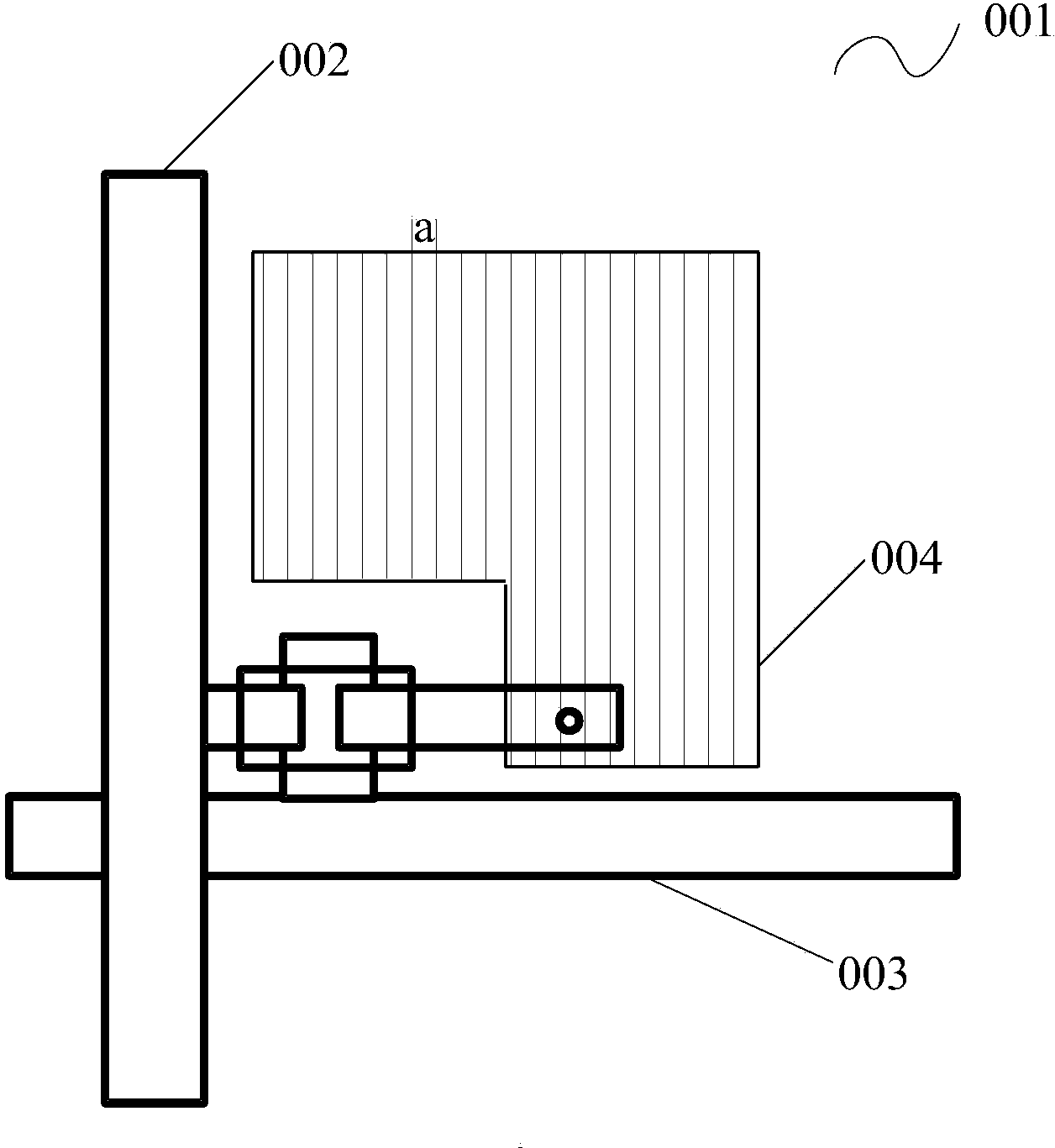
[0039] In this example, if Figure 2a and Figure 2b As shown, the pixel electrode and the wire grid polarizing film are multiplexed in the array substrate. Specifically, the wire grid polarizing film 004 is multiplexed as a pixel electrode in each pixel area, and is electrically connected to the drain 005 of the thin film transistor disposed at the intersection of the data line 002 and the gate line 003. The drain 005 is generally connected to the data line 002 Same level settings.
[0040] Specifically, when the wire grid polarizing film 004 is arranged on the same layer as the data line 002, as Figure 2aAs shown, at this time, since the wire grid polarizing film 004 serving as the pixel electrode is fabricated on the same layer as the drain 005 of the thin film transistor, the two can be directly electrically connected. When the wire grid polarizing film 004 is set on the same layer as the grid line 003, as Figure 2b As shown, at this time, the wire grid polarizing fi...
Embodiment 2
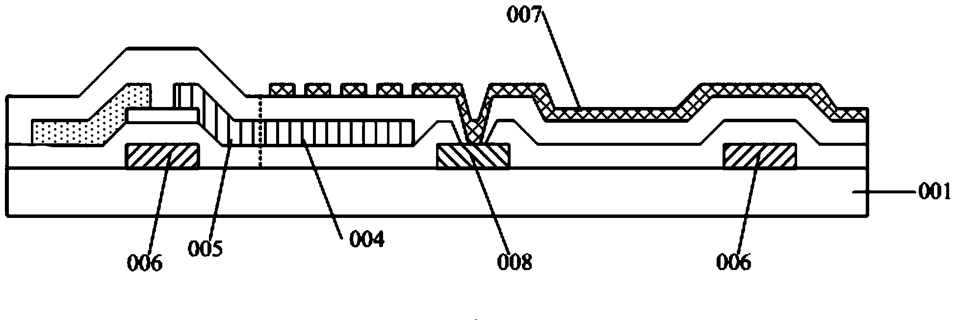
[0045] In this example, if Figure 3a and Figure 3b As shown, the pixel electrodes and common electrodes in the array substrate in the IPS mode are multiplexed with the wire grid polarizing film. Specifically, in the structure of the array substrate in the IPS mode, the pixel electrode and the common electrode in each pixel unit are arranged on the same layer in an interleaved finger structure. Therefore, in each pixel area, the wire grid polarizing film 004 is multiplexed as the pixel electrode and the common electrode of the interpolation structure; wherein, the wire grid polarizing film 004 multiplexed as the pixel electrode and the wire grid polarizing film 004 disposed at the intersection of the data line 002 and the gate line 003 The drain 005 of the TFT is electrically connected, and the drain 005 and the data line 002 are arranged on the same layer.
[0046] Specifically, when the wire grid polarizing film 004 is arranged on the same layer as the data line 002, as ...
Embodiment 3
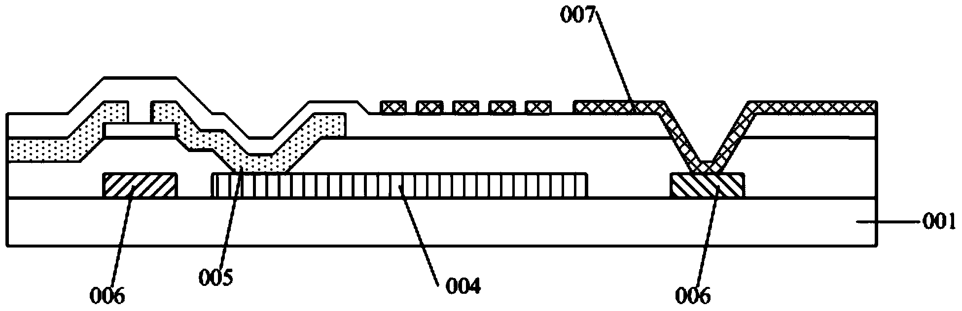
[0050] In this example, if Figure 4 As shown, the pixel electrode and the wire grid polarizing film are multiplexed in the array substrate. Specifically, the wire grid polarizing film 004 and the grid lines 003 can be provided on the same layer, and the wire grid polarizing film 004 can be multiplexed as a common electrode in each pixel area.
[0051] In actual implementation, when making Figure 4 In the case of the ADS type array substrate with the structure shown, the wire grid polarizing film 004 used as the common electrode is set to be fabricated simultaneously with the grid line 003 and the grid 006, so that the existing common electrode formed separately on the pixel electrode can be omitted. Therefore, compared with the existing array substrate manufacturing process, the number of mask plates used and the manufacturing process can be saved.
PUM
 Abstract
Description
Claims
Application Information
 - R&D
- Intellectual Property
- Life Sciences
- Materials
- Tech Scout
- Unparalleled Data Quality
- Higher Quality Content
- 60% Fewer Hallucinations
Browse by: Latest US Patents, China's latest patents, Technical Efficacy Thesaurus, Application Domain, Technology Topic, Popular Technical Reports.
© 2025 PatSnap. All rights reserved.Legal|Privacy policy|Modern Slavery Act Transparency Statement|Sitemap|About US| Contact US: help@patsnap.com