Stackable sensor chip structure and preparation method thereof

A sensor chip and stacking technology, which is applied in the field of stacked sensor chip structure and its preparation, can solve the problems of small photosensitive area and weak isolation of pixels, and achieve the effects of improving shooting effect, increasing area, and improving photosensitive performance

Inactive Publication Date: 2015-02-04
OMNIVISION TECH (SHANGHAI) CO LTD
View PDF7 Cites 2 Cited by
  • Summary
  • Abstract
  • Description
  • Claims
  • Application Information

AI Technical Summary

Problems solved by technology

[0007] In view of the above existing problems, the present invention discloses a stacked sensor chip structure and its preparation method to overcome the small area of ​​the pixel photosensitive are

Method used


Image

  • Stackable sensor chip structure and preparation method thereof
  • Stackable sensor chip structure and preparation method thereof
  • Stackable sensor chip structure and preparation method thereof

Examples


Embodiment Construction

[0043] The present invention will be further described below in conjunction with the accompanying drawings and specific embodiments, but not as a limitation of the present invention.

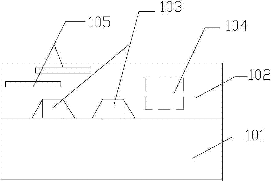
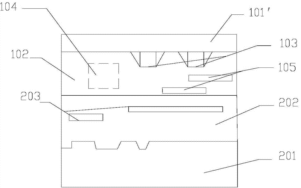
[0044] Figure 9 It is a schematic structural diagram of a stacked sensor chip in an embodiment of the present invention; as Figure 9 Shown:

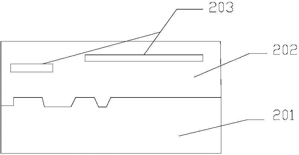
[0045] This embodiment relates to a stacked sensor chip structure, which can be applied to 2T, 4T and 8T image sensors or other pixel area structures, specifically including: a logic device wafer 2 and a conversion layer covering the upper surface of the logic device wafer 2 A device wafer 3 and an inverted pixel device wafer 1 covering the upper surface of the conversion device wafer 3; a plurality of transmission gates 13 are arranged on the pixel device wafer 1, and a row selection device 35 is arranged on the conversion device wafer 2 , a source follower device 34 and a reset device 33; the gate of the source follower device 34 and the drain of the...


PUM

PropertyMeasurementUnit
Thicknessaaaaaaaaaa

Abstract

The invention discloses a stackable sensor chip structure and a preparation method thereof. Through adding a converter wafer between a pixel device wafer and a logic device wafer, areas originally for accommodating a column selector, a source electrode follower and a resetting device on the pixel device wafer are cleared out so that the area of a pixel photosensitive region is increased and the photosensitive performance of the chip is improved. Therefore, the shooting effect under a low-illumination condition is improved and isolation of pixel-area transmission gratings and the column selector, the source electrode follower and the resetting device is strengthened and thus parameters such as dark current and noise and the like are reduced. The stackable sensor chip structure is scientific and reasonable in design, high in compatibility with a traditional technology and easy to realize.

Description

technical field [0001] The invention relates to the technical field of semiconductor manufacturing, in particular to a stacked sensor chip structure and a preparation method thereof. Background technique [0002] At present, there are many ways to improve the photosensitive performance of the chip. The stacked sensor chip itself is an improvement based on the ordinary back-illuminated sensor chip. It increases the pixel area without increasing the chip area, thereby improving the photosensitive performance of the chip. Performance, the stacked sensor chip is bonded by two wafers with different structures. One piece is a pixel device wafer, including a pixel device substrate 101, a pixel device dielectric layer 102 covering the surface of the pixel device substrate 101, a transmission gate 103 arranged in the pixel device dielectric layer 102, a conversion device 104 (including a row selection device , source follower device and reset device) and pixel device metal wiring la...

Claims


Application Information

Patent Timeline
IPC IPC(8): H01L27/146
Inventor 林峰肖海波刘远良
Owner OMNIVISION TECH (SHANGHAI) CO LTD
Why Eureka
Try Eureka