Semiconductor device and method for producing same

A manufacturing method and semiconductor technology, which are applied in the direction of semiconductor devices, semiconductor/solid-state device components, electric solid-state devices, etc., to achieve the effects of high heat dissipation, large occupation area, and small thermal resistance

Inactive Publication Date: 2015-02-04
PANASONIC INTELLECTUAL PROPERTY MANAGEMENT CO LTD
View PDF2 Cites 1 Cited by
  • Summary
  • Abstract
  • Description
  • Claims
  • Application Information

AI Technical Summary

Problems solved by technology

For example, the efficiency of high-efficiency GaN and SiC used in high-output control semiconductors for motors is about 98%, but about 2% becomes heat, which will become a problem in the process of using at high output

Method used


Image

  • Semiconductor device and method for producing same
  • Semiconductor device and method for producing same
  • Semiconductor device and method for producing same

Examples


Embodiment Construction

[0061] Hereinafter, the semiconductor device and its manufacturing method of the present invention will be described in detail. In addition, various elements shown in the drawings are merely schematically shown for understanding the present invention, and it should be noted that dimensional ratios, appearances, etc. may be different from actual ones.

[0062] [Semiconductor device of the present invention]

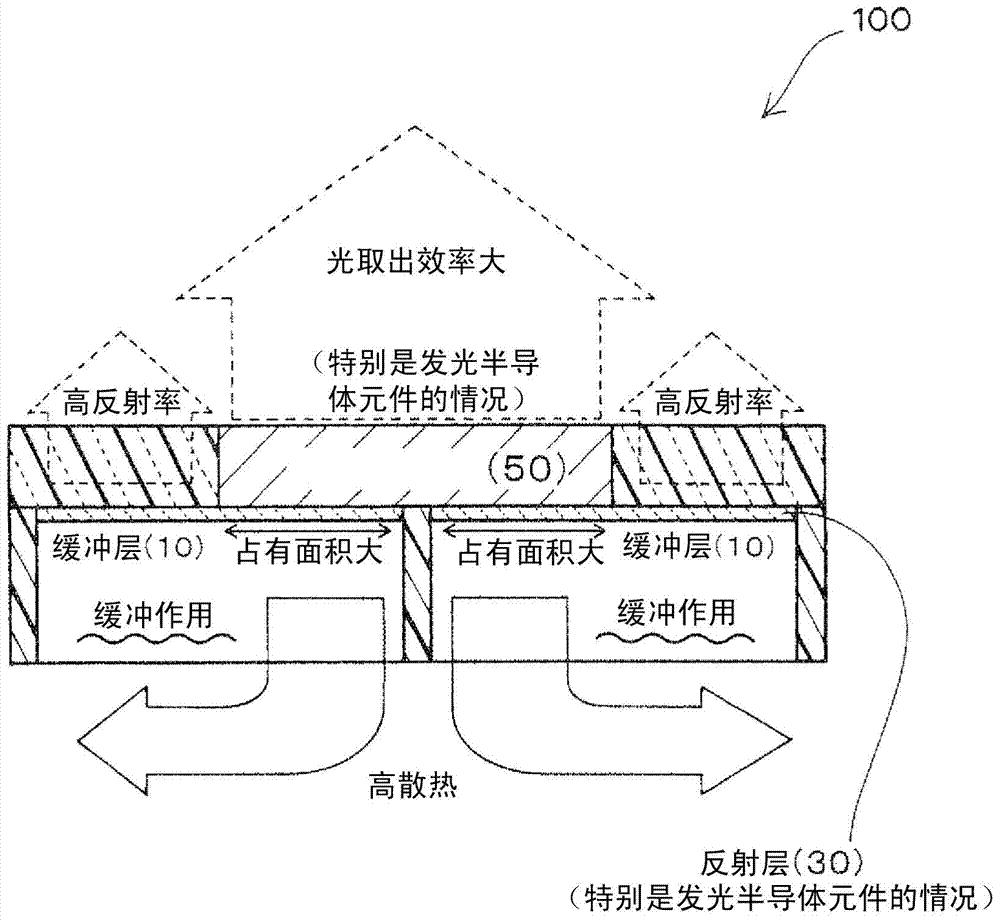
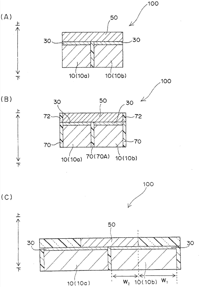
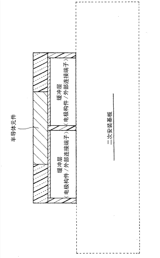
[0063] exist figure 2 (A) to (C) schematically show the configuration of the semiconductor device of the present invention. As shown in the figure, the semiconductor device 100 of the present invention includes a metal buffer layer 10 , a metal buffer layer substrate 30 and a semiconductor element 50 . The semiconductor element 50 has a form provided on the metal buffer layer 10 and is provided in contact with at least a part of the base 30 on the metal buffer layer. The metal buffer layer 10 is used as an external connection terminal (such as an electrode member of a ...


PUM


Abstract

This semiconductor device includes a semiconductor element and a metal buffer layer electrically connected to the semiconductor element. In this semiconductor device, the metal buffer layer and the semiconductor element are connected with each other in such a form that the metal buffer layer and the semiconductor element are in surface contact with each other. Further, the metal buffer layer functions as an external connection terminal used for the mounting onto a secondary mount substrate, and at the same time, also functions as a buffer member that provides an effect of reducing a stress between the secondary mount substrate and the semiconductor element.

Description

technical field [0001] The present invention relates to a semiconductor device and its manufacturing method. More specifically, the present invention relates to a semiconductor device having excellent heat dissipation and high reliability and a method for manufacturing the same. Background technique [0002] In recent years, semiconductors that control large currents have been used in hybrid vehicles that combine gasoline engines and electric motors. In addition, such semiconductors are also used in the high output current control of electric motors along with the spread of electric vehicles that run only with electric motors. [0003] Furthermore, a semiconductor (LED) that emits light as a light source is used in various applications because of its energy saving and long life. For example, LEDs are used in various lighting applications in addition to applications such as backlight sources for display devices (liquid crystal screens), camera flash applications, and automo...

Claims


Application Information

Patent Timeline
Patent Type & Authority Applications(China)
IPC IPC(8): H01L23/12H01L23/28H01L23/36H01L33/62H01L33/64
CPCH01L2224/05669H01L2224/05639H01L24/96H01L2224/96H01L2224/0346H01L23/562H01L24/94H01L2224/97H01L24/05H01L2924/12041H01L24/03H01L2224/04105H01L2224/05647H01L33/647H01L2224/05567H01L2224/49107H01L23/3677H01L2224/48091H01L2224/05655H01L2224/94H01L2224/05664H01L2924/13055H01L2924/00014H01L2224/04042H01L2924/351H01L2924/15747H01L2924/15787H01L2224/45144H01L2224/48639H01L2224/48647H01L2224/48655H01L2224/48664H01L2224/48669H01L2924/12042H01L2924/181H01L2224/14H01L33/60H01L2933/0058H01L2933/0075H01L2224/73267H01L2224/82H01L2224/03H01L2924/00015H01L2924/00H01L2224/05552H01L2924/00012H01L24/27H01L24/32H01L24/83H01L2224/2746H01L2224/2784H01L2224/32113H01L2224/3224H01L2224/3226H01L2924/2064H01L2924/2075H01L2933/0066
Inventor 川北晃司泽田享中谷诚一山下嘉久
Owner PANASONIC INTELLECTUAL PROPERTY MANAGEMENT CO LTD
Why Eureka
Try Eureka