Fixing plugboard for printed circuit board

A technology of printed circuit boards and plug-in boards, which is applied in the direction of printed circuits, printed circuit manufacturing, and assembly of printed circuits with electrical components, and can solve problems affecting quality and production efficiency, large hollowing of printed circuit boards, and offline printing of printed circuit boards. , to achieve the effect of avoiding rushing to the top surface of the printed circuit board, avoiding offline, and reducing deformation

Inactive Publication Date: 2015-02-11
GREE ELECTRIC APPLIANCES INC
View PDF9 Cites 5 Cited by
  • Summary
  • Abstract
  • Description
  • Claims
  • Application Information

AI Technical Summary

Problems solved by technology

[0004] At present, when some printed circuit boards pass through the wave furnace, due to reasons such as large and thin printed circuit boards or many hollows, the printed circuit boards are heated and deformed in the preheating section of the wave furnace, and the middle is sunken. If it is not serious, it will also face the danger of molten solder rushing to the top surface of the printed circuit board when passing the peak of the tin flow, which will cause a large number of printed circuit boards to go offline, seriously affecting the quality and production efficiency

Method used


Image

  • Fixing plugboard for printed circuit board
  • Fixing plugboard for printed circuit board
  • Fixing plugboard for printed circuit board

Examples


Embodiment Construction

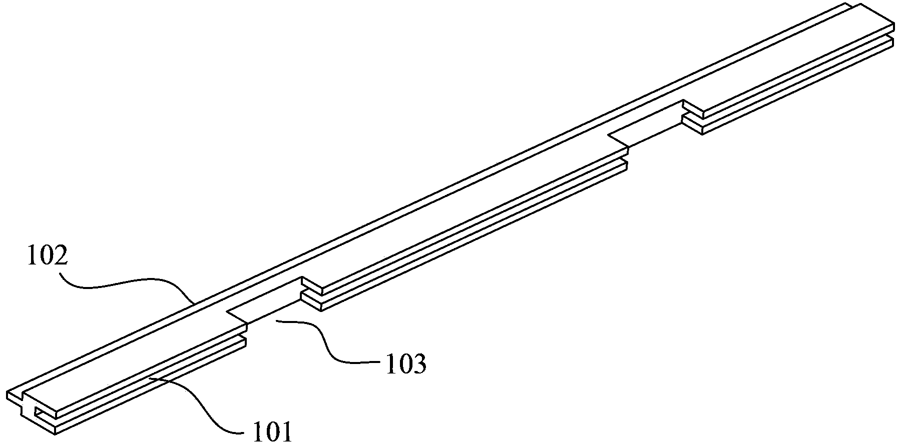
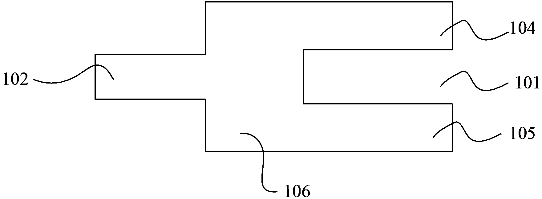
[0034] The core of the present invention is to provide a fixed board for a printed circuit board, so as to avoid deformation of the printed circuit board when passing through a wave furnace.

[0035] The following will clearly and completely describe the technical solutions in the embodiments of the present invention with reference to the accompanying drawings in the embodiments of the present invention. Obviously, the described embodiments are only some, not all, embodiments of the present invention. Based on the embodiments of the present invention, all other embodiments obtained by persons of ordinary skill in the art without making creative efforts belong to the protection scope of the present invention.

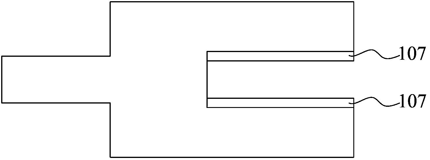
[0036] see figure 1 with figure 2 , figure 1 A schematic structural diagram of a fixed board for a printed circuit board provided by an embodiment of the present invention; figure 2 It is a side view of a fixed board for a printed circuit board provided by an embodi...


PUM


Abstract

The invention discloses a fixing plugboard for a printed circuit board. The fixing plugboard comprises a plugboard body, the plugboard body is provided with a slot, and the width of the slot is adaptive to the thickness of the printed circuit board. According to the fixing plugboard for the printed circuit board, provided by the invention, the plugboard body is provided with the slot for clamping the printed circuit board, when the printed circuit board passes through a peak furnace, the fixing plugboard is pressed to at least one side of the printed circuit board, the slot of the fixing plugbaord and the edge of the printed circuit board cooperate in a clamping mode so as to be fixed together, thus deformation is reduced. Before furnace operation, the fixing plugboard is pressed to the at least one side of the printed circuit board, the printed circuit board can be fixed, deformation due to heating of the printed circuit board is prevented, the risk of falling off from the conveying track of the peak furnace is avoided, and the risk of fusion soldering tin rushing to the top surface of the printed circuit board is also avoided, such that the problem that a lot of printed circuit boards are took out from a production line is prevented, and the quality of the printed circuit board and the production efficiency are improved.

Description

technical field [0001] The invention relates to the technical field of wave soldering of circuit boards, and more specifically relates to a fixed plug-in board for printed circuit boards. Background technique [0002] Wave soldering is a soft soldering method, which drives the molten solder upward through a mechanical pump or electromagnetic pump, and the jet flow forms a solder wave peak that meets the design requirements, and makes the printed circuit board pre-installed with electronic components to be soldered The surface passes through the solder wave crest, so that the electrical connection between the solder terminal or pin of the electronic component exposed on the surface of the printed circuit board to be soldered and the pad of the printed circuit board is realized. [0003] The process of soldering printed circuit boards by wave soldering process is: the printed circuit board contacts the tin flow peak formed in the wave furnace with the surface of the printed ci...

Claims


Application Information

Patent Timeline
Patent Type & Authority Applications(China)
IPC IPC(8): H05K3/34
CPCH05K3/34H05K2203/1545
Inventor 孙超刘桂陈斌伍小途李路
Owner GREE ELECTRIC APPLIANCES INC
Why Eureka
Try Eureka