Printed circuit board and manufacturing method thereof

A technology for printed circuit boards and manufacturing methods, which is applied in the fields of printed circuit manufacturing, printed circuits, printed circuits, etc., and can solve problems such as shrapnel topping

Inactive Publication Date: 2015-02-11
SHENZHEN GONGJIN ELECTRONICS CO LTD
View PDF4 Cites 2 Cited by
  • Summary
  • Abstract
  • Description
  • Claims
  • Application Information

AI Technical Summary

Problems solved by technology

[0004] Based on this, it is necessary to provide a method of manufacturing a printed circuit board for the problem that the tin surface on the pad is easy to push the shrapnel when the traditional printed circuit board is in contact with the shrapnel.

Method used


Image

  • Printed circuit board and manufacturing method thereof
  • Printed circuit board and manufacturing method thereof
  • Printed circuit board and manufacturing method thereof

Examples


Embodiment Construction

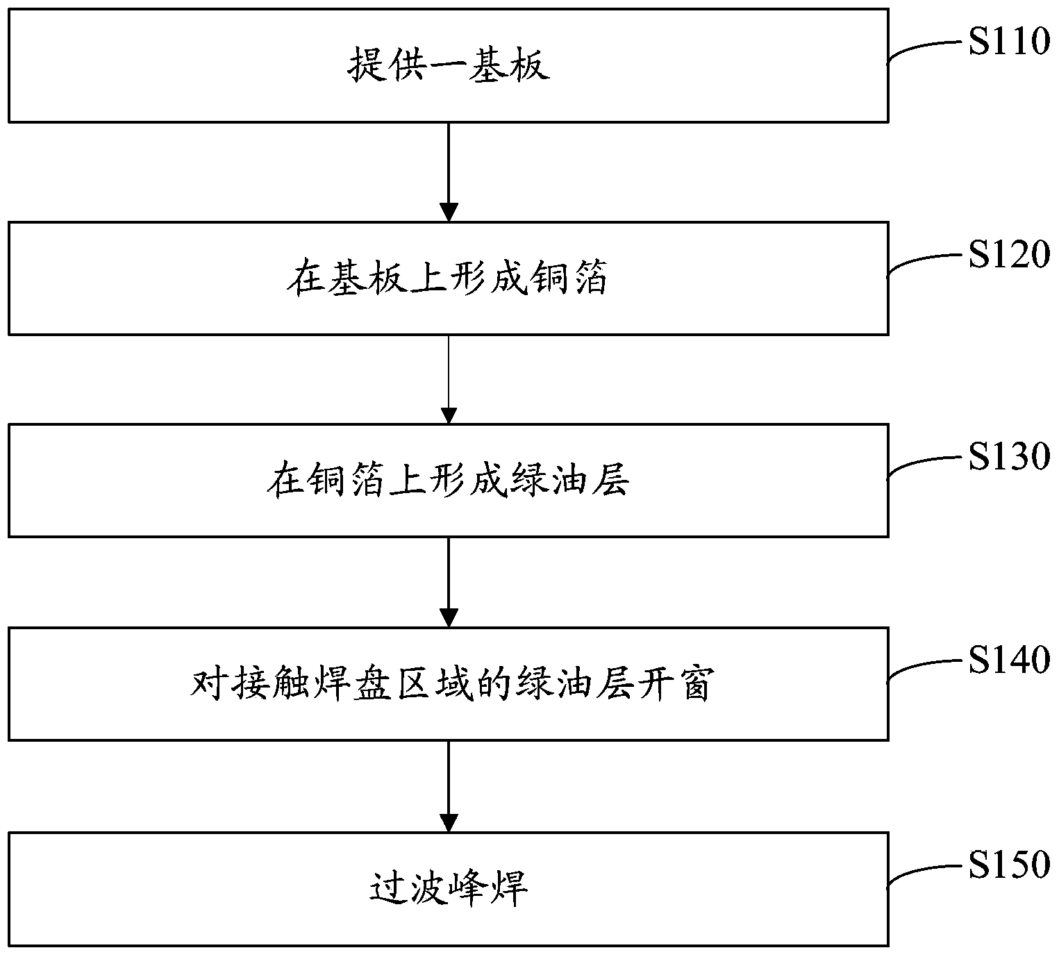
[0017] The invention aims at the problem that the tin surface on the welding pad is easy to push the shrapnel when the traditional printed circuit board is in contact with the shrapnel, and provides a method for manufacturing the printed circuit board.

[0018] In order to facilitate the understanding of the present invention, the present invention will be described more fully below with reference to the associated drawings. A preferred embodiment of the invention is shown in the drawings. However, the present invention can be embodied in many different forms and is not limited to the embodiments described herein. Rather, these embodiments are provided so that the disclosure of the present invention will be thorough and complete.

[0019] It should be noted that when an element is referred to as being “fixed” to another element, it can be directly on the other element or there can also be an intervening element. When an element is referred to as being "connected to" another ...


PUM


Abstract

The invention discloses a manufacturing method of a printed circuit board. The manufacturing method comprises the following steps: providing a substrate; forming a copper foil on the substrate; forming a green oil layer on the surface of the copper foil; windowing the green oil layers of at least one contact bonding pad regions, wherein each contact bonding pad region corresponds to one shrapnel and multiple subwindows are formed each contact bonding pad region in the windowing step; performing wave soldering so as to form tin ingots with shapes similar to those of the subwindows, wherein the tin ingots of each contact bonding pad region form a contact bonding pad electrically with the shrapnel. The invention further discloses a printed circuit board. The contact welding pan consists of multiple tin ingots, i.e., the tin ingot area is reduced, so that the tin of the tin ingots is uniform and even, and the tin ingots can be effectively contacted with the shrapnels; the arc height of a tin surface is controlled below 0.2mm, and normal installation of the shrapnels is not influenced.

Description

technical field [0001] The invention relates to the field of printed circuits, in particular to a printed circuit board and a manufacturing method thereof. Background technique [0002] For power adapters, the plug is usually connected with a wire and a printed circuit board. Due to the miniaturization of the equipment and in order to simplify the installation procedure, some power adapters have been changed to shrapnel. [0003] When changing to the shrapnel mode, the printed circuit board contacts the shrapnel through the pad to form an electrical connection. In the actual design process, in order to ensure the effective contact between the shrapnel and the printed circuit board, the designer does not give much room for expansion and contraction of the shrapnel itself. The inventor found in actual production and use that when installing the shrapnel, the tin surface on the pad is likely to push the shrapnel to death, resulting in problems in installation. Contents of t...

Claims


Application Information

Patent Timeline
Patent Type & Authority Applications(China)
IPC IPC(8): H05K3/34H05K1/11
CPCH05K1/11H05K3/403H05K2201/09409H05K2201/09427
Inventor 王达国
Owner SHENZHEN GONGJIN ELECTRONICS CO LTD
Why Eureka
Try Eureka