Circuit substrate, memory chip and imaging box

A circuit substrate and substrate technology, applied in the directions of printed circuits, printed circuits, printed circuit components, etc., can solve the problems of unstable contact between elastic electrodes and circuit substrates, unstable electrical connection of circuit substrates, etc., to avoid influence and improve contact. Good performance and stability

Active Publication Date: 2015-02-25
APEX MICROELECTRONICS CO LTD
View PDF4 Cites 6 Cited by
  • Summary
  • Abstract
  • Description
  • Claims
  • Application Information

AI Technical Summary

Problems solved by technology

[0005] The invention provides a circuit substrate, a memory chip and an imaging box, which are used to solve the technical defects in the prior art that the contact between the elastic electrode and the circuit substrate is unstable, and the electrical connection with the circuit substrate is unstable

Method used


Image

  • Circuit substrate, memory chip and imaging box
  • Circuit substrate, memory chip and imaging box
  • Circuit substrate, memory chip and imaging box

Examples


Embodiment Construction

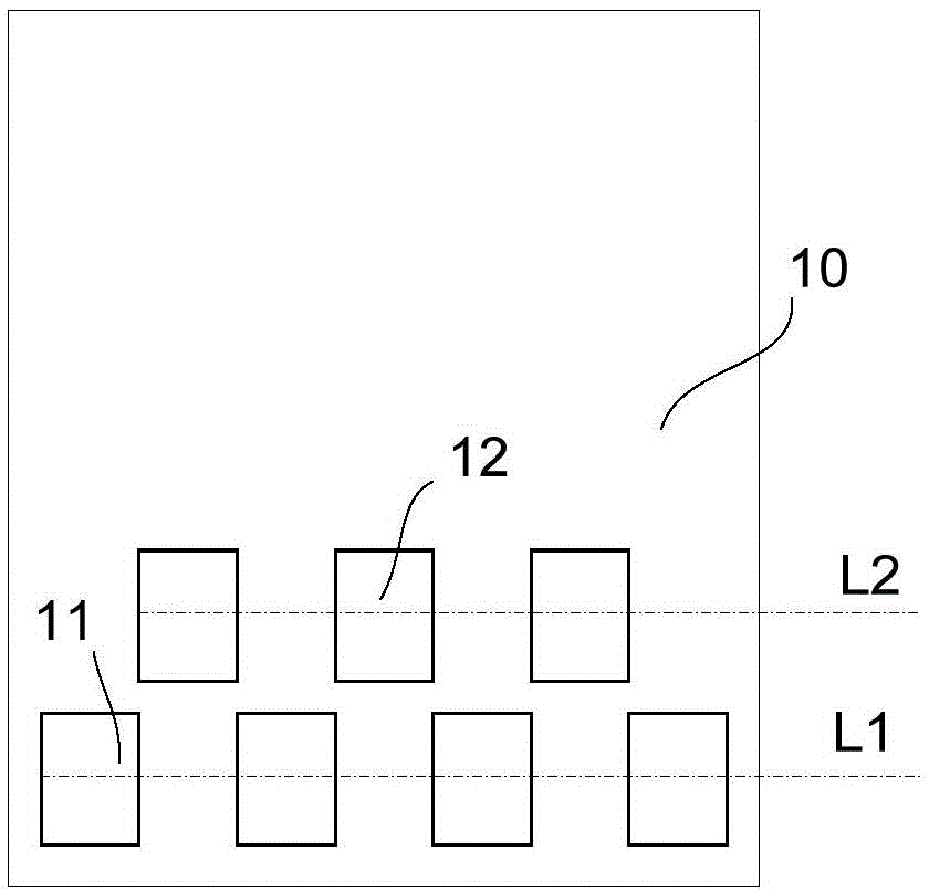
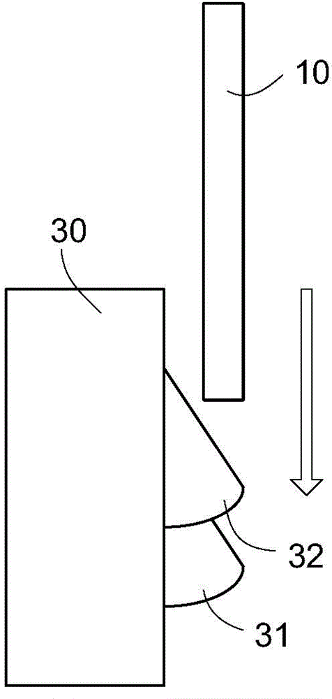
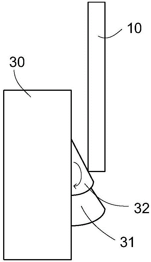
[0030] image 3 Schematic diagram of the hard board structure of the circuit substrate provided by the embodiment of the present invention; Figure 4 A schematic diagram of the structure of the circuit substrate provided by the embodiment of the present invention before it is installed on the printer; Figure 5 Schematic diagram of the structure of the circuit substrate provided by the embodiment of the present invention after it is installed on the printer; Figures 6a-6b for Figure 4 Schematic diagram of the installation process of the shown circuit substrate and the second row of elastic electrodes of the printer; Figure 7a-7b for Figure 4 Schematic diagram of the installation process of the shown circuit substrate and the first row of elastic electrodes of the printer; Figure 8 It is a schematic diagram of the circuit substrate provided by the embodiment of the present invention after it is installed in the printer.

[0031] Such as Figure 3-8 As shown, the circ...


PUM


Abstract

The invention relates to a circuit substrate, a memory chip and an imaging box. The circuit substrate comprises a hard board and multiple signal ends, wherein the multiple signal ends are arranged in a staggered mode and respectively form, at least, a first row of signal ends and a second row of signal ends which are close to each other. The circuit substrate is characterized by comprising at least one flexible board, wherein one section of the flexible board is fixedly connected with the hard board, the other section of the flexible board is a free section, at least one of the multiple signal ends is arranged at the free section of the flexible board, and grooves are formed in the hard board portion corresponding to the signal ends arranged at the free section of the flexible board. Due to the fact that the grooves are formed in the circuit substrate, elastic electrodes of an imaging device extrude the flexible board portion where the signal ends are located in the contact process of the elastic electrode and the signal ends, the flexible board where the signal ends are located deforms, finally the elastic electrodes are clamped in the grooves and are kept to be electrically connected with the signal ends, electrical connection stability is good, even the influence of dust or oxides on electrical connection can be further reduced, and the contact performance of a circuit is improved.

Description

technical field [0001] The present invention relates to imaging equipment technology, such as printer technology, copier technology and facsimile machine technology, especially relates to circuit substrate, storage chip and imaging box. Background technique [0002] The ink cartridge of the existing inkjet printer is provided with a memory chip, figure 1 It is a schematic structural diagram of an existing circuit substrate; such as figure 1 As shown, the circuit substrate 10 of the existing memory chip is roughly rectangular, and various components of the memory chip are arranged on the circuit substrate 10, and a plurality of substantially rectangular signal terminals are arranged on one surface of the circuit substrate 10, A plurality of signal terminals are arranged in a staggered manner on the circuit substrate 10, respectively forming a first row of signal terminals 11 and a second row of signal terminals 12, corresponding to figure 1 In L1 and L2, the above-mentioned...

Claims


Application Information

Patent Timeline
Patent Type & Authority Applications(China)
IPC IPC(8): H05K1/11
CPCH05K1/117H05K1/118H05K2201/09072
Inventor 李博曾梅莲钟坚陈琪唐笑贤
Owner APEX MICROELECTRONICS CO LTD
Why Eureka
Try Eureka