Method for forming totally-enclosed gate structure

A technology of fully surrounding gates and gate dielectrics, which is applied in the direction of electrical components, semiconductor/solid-state device manufacturing, semiconductor devices, etc., can solve the problems of high cost and complicated process, and achieve the effect of low cost, simple method and easy implementation

Active Publication Date: 2015-03-04
SHANGHAI INTEGRATED CIRCUIT RES & DEV CENT
View PDF5 Cites 8 Cited by
  • Summary
  • Abstract
  • Description
  • Claims
  • Application Information

AI Technical Summary

Problems solved by technology

[0013] The purpose of the present invention is to overcome the above-mentioned defects in the prior art, and provide a method for forming a fully-enclosed gate structure, which is used to manufacture FinFET devices. The gate dielectric, Fin, and gate are formed step by step by using a planar process, and the surrounding Fin The lower end of the grid is connect

Method used


Image

  • Method for forming totally-enclosed gate structure
  • Method for forming totally-enclosed gate structure
  • Method for forming totally-enclosed gate structure

Examples


Embodiment Construction

[0033] The specific embodiment of the present invention will be further described in detail below in conjunction with the accompanying drawings.

[0034] It should be noted that, in the following specific embodiments, when describing the embodiments of the present invention in detail, in order to clearly show the structure of the present invention for the convenience of description, the structures in the drawings are not drawn according to the general scale, and are drawn Partial magnification, deformation and simplification are included, therefore, it should be avoided to be interpreted as a limitation of the present invention.

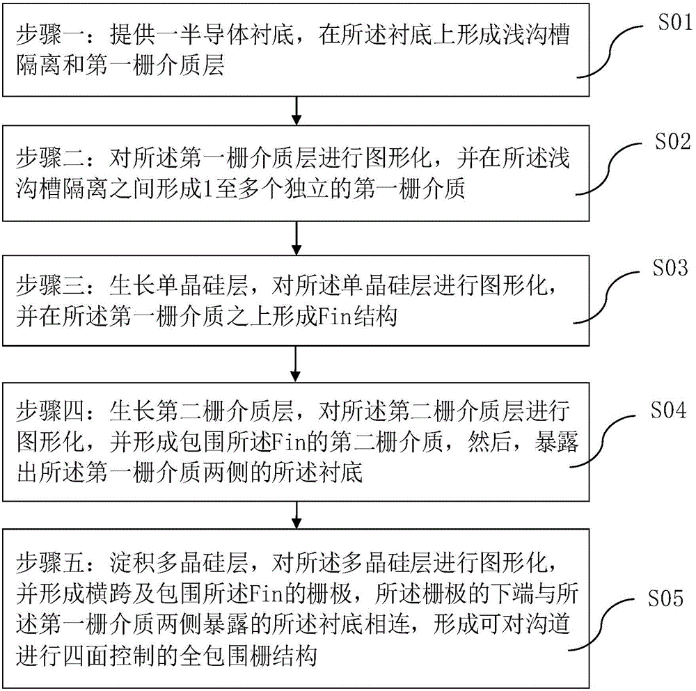
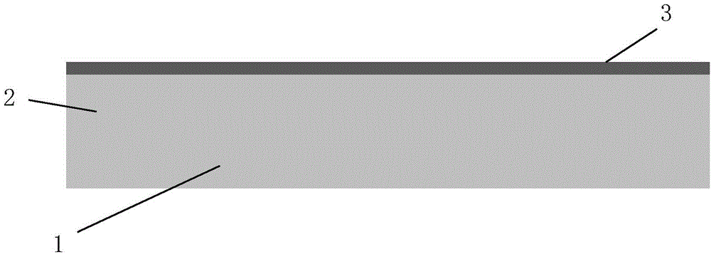
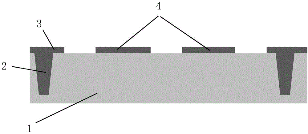
[0035] In this example, see figure 1 , figure 1 It is a flow chart of a method for forming a fully enclosed gate structure in the present invention; meanwhile, please refer to Figure 2 to Figure 9 , Figure 2 to Figure 9 is the application figure 1 A schematic diagram of the device structure of an embodiment of an all-enclosed gate structure of ...


PUM

PropertyMeasurementUnit
Thicknessaaaaaaaaaa
Widthaaaaaaaaaa
Thicknessaaaaaaaaaa

Abstract

The invention discloses a method for forming a totally-enclosed gate structure. The method is used for manufacturing FinFET devices, and comprises forming a gate dielectric, Fin and a gate in steps by use of a planar process and connecting the lower end of the gate surrounding the Fin with a substrate to form the totally-enclosed gate structure. As the gate dielectric is quite thin and the lower end of the gate is connected with the substrate, the gate is enabled to effectively control channels from all sides still in a totally enclosing form. As a result, the method for forming the totally-enclosed gate structure succeeds in solving the problems of complex process and high cost in the prior art while guaranteeing the desired device characteristics. The method is simple and convenient, and compatible with the existing integrated circuit planar process, and has the advantages of low cost, easy implementation and the like.

Description

technical field [0001] The present invention relates to the technical field of manufacturing technology of semiconductor integrated circuits, and more particularly, relates to a method for forming a complex all-enclosed gate structure with a relatively simple process for manufacturing FinFET devices. Background technique [0002] The semiconductor integrated circuit (IC) industry has undergone rapid development. During the development of ICs, functional density (i.e., the number of interconnected devices per chip area) has generally increased while geometry size (i.e., the smallest device or interconnect line that can be made using a fabrication process) has decreased. The advantages of this scaled-down process are increased production efficiency and reduced associated costs. At the same time, this scaled-down process also increases the complexity of handling and manufacturing ICs. [0003] In the process of seeking higher device density, higher performance, and lower cost...

Claims


Application Information

Patent Timeline
IPC IPC(8): H01L21/28
CPCH01L21/28035H01L29/66795
Inventor 储佳
Owner SHANGHAI INTEGRATED CIRCUIT RES & DEV CENT
Why Eureka
Try Eureka