High-resolution OLED device and masking plate for manufacturing same

A high-resolution and device technology, which is applied in semiconductor/solid-state device manufacturing, electric solid-state devices, semiconductor devices, etc., can solve the problems that it is difficult to make high-resolution OLED panels, and achieve improved aperture ratio, clear display, The effect of reducing the requirements of the process technology

Inactive Publication Date: 2015-03-04
SICHUAN CCO DISPLAY TECH
View PDF8 Cites 13 Cited by
  • Summary
  • Abstract
  • Description
  • Claims
  • Application Information

AI Technical Summary

Problems solved by technology

[0003] The purpose of the present invention is to solve the problem that the existing OLED pixel arrangement structure is produced by using the existing manufacturing process, due to the difficulty of mask processing and alignment accuracy, it is difficult to make a high-resolution OLED panel, and proposes A high-resolution OLED device that can reduce the limitation on the processing precision of the mask plate and a mask plate dedicated to the manufacture of the OLED device

Method used


Image

  • High-resolution OLED device and masking plate for manufacturing same
  • High-resolution OLED device and masking plate for manufacturing same
  • High-resolution OLED device and masking plate for manufacturing same

Examples


Embodiment Construction

[0022] The following embodiments of the present invention are designed according to the principles of the present invention. The protection scope of the technical solution of the present invention includes but is not limited to the scope of the following specific embodiments. The present invention will be further elaborated below in conjunction with the accompanying drawings and specific embodiments.

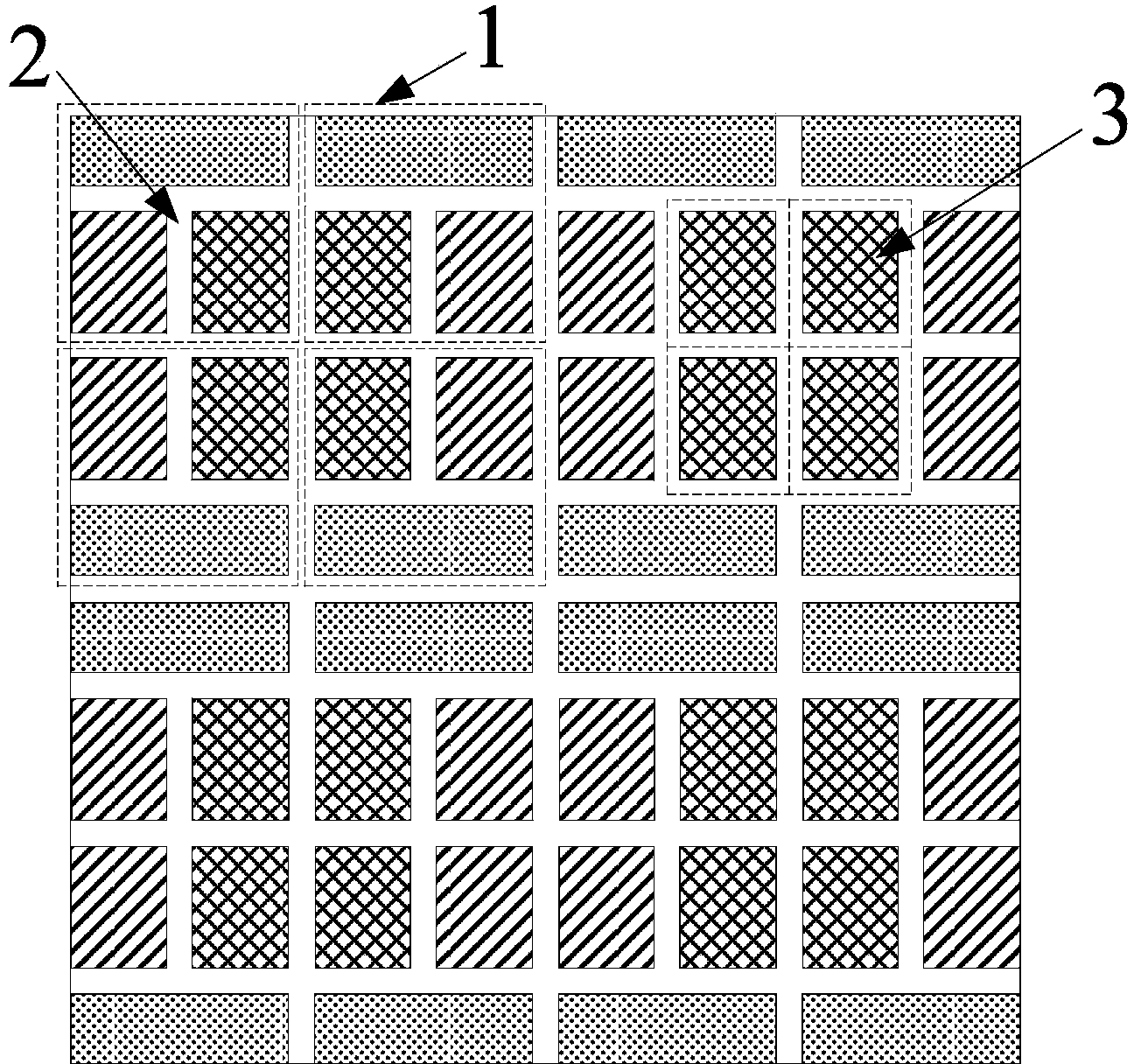
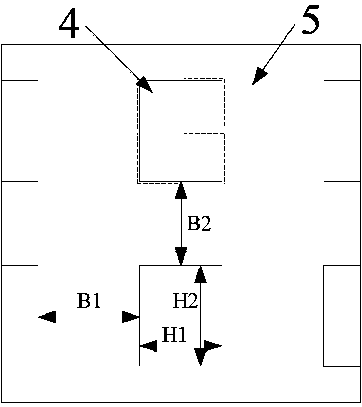
[0023] Such as figure 2 As shown, a high-resolution OLED device of this embodiment includes pixel groups 1 arranged in a matrix, a single pixel group 1 includes four pixels 2, and a single pixel 2 includes red, green, and blue sub-pixels; The three-color sub-pixels of red, green, and blue are arranged in a pixel in a square shape, and the red, green, and blue three-color sub-pixels of adjacent pixels in the pixel group are symmetrical about the common edge of the pixel.

[0024] The four pixels 2 in the pixel group 1 are arranged in a square shape, and the four pixels 2 in the ...


PUM


Abstract

A high-resolution OLED device comprises pixel units which are distributed into matrixes, each pixel unit comprises four pixels, and each pixel comprises a red sub-pixel, a green sub-pixel and a blue sub-pixel; each red sub-pixel, the corresponding green sub-pixel and the corresponding blue sub-pixel are distributed in a shape like a Chinese character 'pin' in the corresponding pixel, and the red sub-pixels, the green sub-pixels and the blue sub-pixels of every two adjacent pixels in each pixel unit are symmetrical with respect to the public edge of the corresponding pixels. The high-resolution OLED device has the advantages that a manufacturing method is based on the proven FMM technique in the industry, but according to the special pixel distribution mode, a MASK evaporated with organic light-emitting materials is in a mesh shape, and each open hole corresponds to four sub-pixels. Under the situation of the same resolution, sizes of the open holes and sizes of connection bridges of the MASK are larger. A high-resolution OLED display screen can be manufactured on the basis the proven FMM technique in the industry; alternatively under the situation of the same resolution, the requirement for MASK processing and OLED display screen manufacturing processes can be reduced, and improvement on the product yield is facilitated.

Description

technical field [0001] The invention belongs to the field of organic light-emitting diode (OLED) display technology, and relates to a pixel arrangement structure of an OLED display panel, in particular to a high-resolution OLED device panel structure and a mask plate for manufacturing the OLED panel. Background technique [0002] Organic Light Emitting Diode (OLED) display is recognized by the industry as the second largest display after Liquid Crystal Display (LCD) due to its thinness, active light emission, fast response speed, wide viewing angle, rich colors and high brightness, low power consumption, high and low temperature resistance and many other advantages. The third-generation display technology can be widely used in terminal products such as smartphones, tablets, and TVs. However, personal mobile products such as smartphones on the market recently put forward higher and higher resolution requirements for display screens. The screen resolution (that is, pixel densi...

Claims


Application Information

Patent Timeline
Patent Type & Authority Applications(China)
IPC IPC(8): H01L27/32H01L51/56C23C14/04
CPCH10K59/352H10K59/353
Inventor 田朝勇郎丰伟
Owner SICHUAN CCO DISPLAY TECH
Why Eureka
Try Eureka