Conformal shielding structure applying lead bonding, and manufacture process thereof
A shielding structure and wire bonding technology, which is applied in the direction of electrical components, electric solid devices, circuits, etc., can solve the problems of unsatisfactory shielding effect, incomplete connection of profiling shielding, etc., achieve the best electrical performance and reduce the packaging cost.
- Summary
- Abstract
- Description
- Claims
- Application Information
AI Technical Summary
Problems solved by technology
Method used
Image
Examples
Embodiment 1
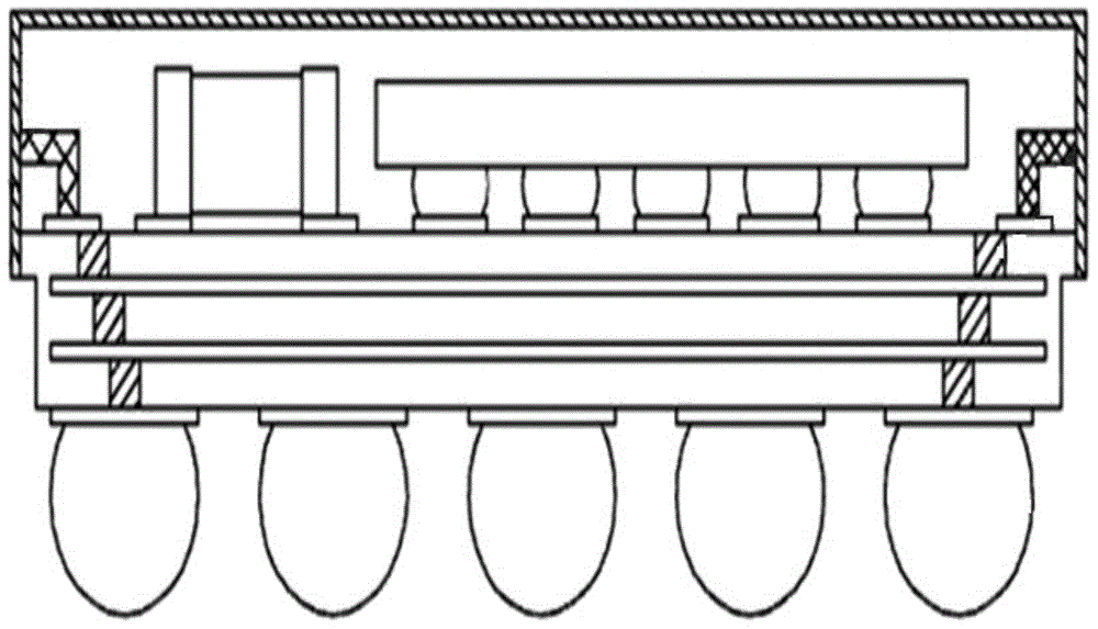
[0032] In this embodiment, the metal layer is a Cu—Co—Si electromagnetic shielding layer with a thickness of about 2.0 μm. The electromagnetic shielding layer is obtained by magnetron sputtering coating, the sputtering target is a Cu-Co-Si composite target, and the mass percentage of Co in the composite target is 32wt%, and the mass percentage of Si is is 3wt%, and the balance is Cu; the sputtering process is: argon is used as the working gas, and its flow rate is 100-200 sccm; the sputtering power is 20kW, and the coating temperature is 50°C.
Embodiment 2
[0034] In this embodiment, the metal layer is a Cu—Co—Si electromagnetic shielding layer with a thickness of about 2.0 μm. The electromagnetic shielding layer is obtained by magnetron sputtering coating, the sputtering target is a Cu-Co-Si composite target, and the mass percentage of Co in the composite target is 35wt%, and the mass percentage of Si is is 6wt%, and the balance is Cu; the sputtering process is: argon is used as the working gas, and its flow rate is 100-200 sccm; the sputtering power is 20kW, and the coating temperature is 50°C.
Embodiment 3
[0036] In this embodiment, the metal layer is a Cu—Co—Si electromagnetic shielding layer with a thickness of about 5.0 μm. The electromagnetic shielding layer is obtained by magnetron sputtering coating, the sputtering target is a Cu-Co-Si composite target, and the mass percentage of Co in the composite target is 32wt%, and the mass percentage of Si is is 3wt%, and the balance is Cu; the sputtering process is: argon is used as the working gas, and its flow rate is 100-200 sccm; the sputtering power is 20kW, and the coating temperature is 50°C.
PUM
 Abstract
Description
Claims
Application Information


