Array Substrate Of Liquid Crystal Display Device

A technology for liquid crystal displays and array substrates, applied in the field of liquid crystal displays, can solve the problems of limited program control capability and the inability to excessively thin the thickness of the insulating layer, and achieve the effects of increasing pixel density, increasing flexibility, and increasing process boundaries

Active Publication Date: 2015-03-18
HONG FU JIN PRECISION IND (SHENZHEN) CO LTD +1
View PDF5 Cites 13 Cited by
  • Summary
  • Abstract
  • Description
  • Claims
  • Application Information

AI Technical Summary

Problems solved by technology

In order to achieve high resolution, the previous technique is to reduce the thickness of the insulating layer. However, due to the limited process control capability, the thickness of the insulating layer cannot be excessively thinned.

Method used


Image

  • Array Substrate Of Liquid Crystal Display Device
  • Array Substrate Of Liquid Crystal Display Device
  • Array Substrate Of Liquid Crystal Display Device

Examples


Embodiment Construction

[0022] An array substrate for a liquid crystal display according to an embodiment of the present invention will be described with reference to the drawings.

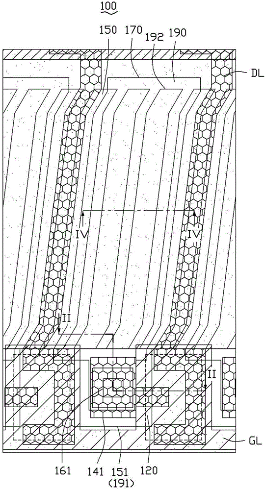
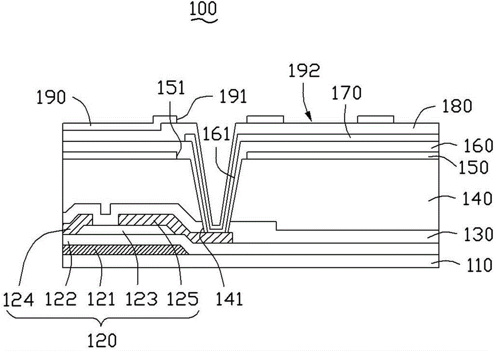
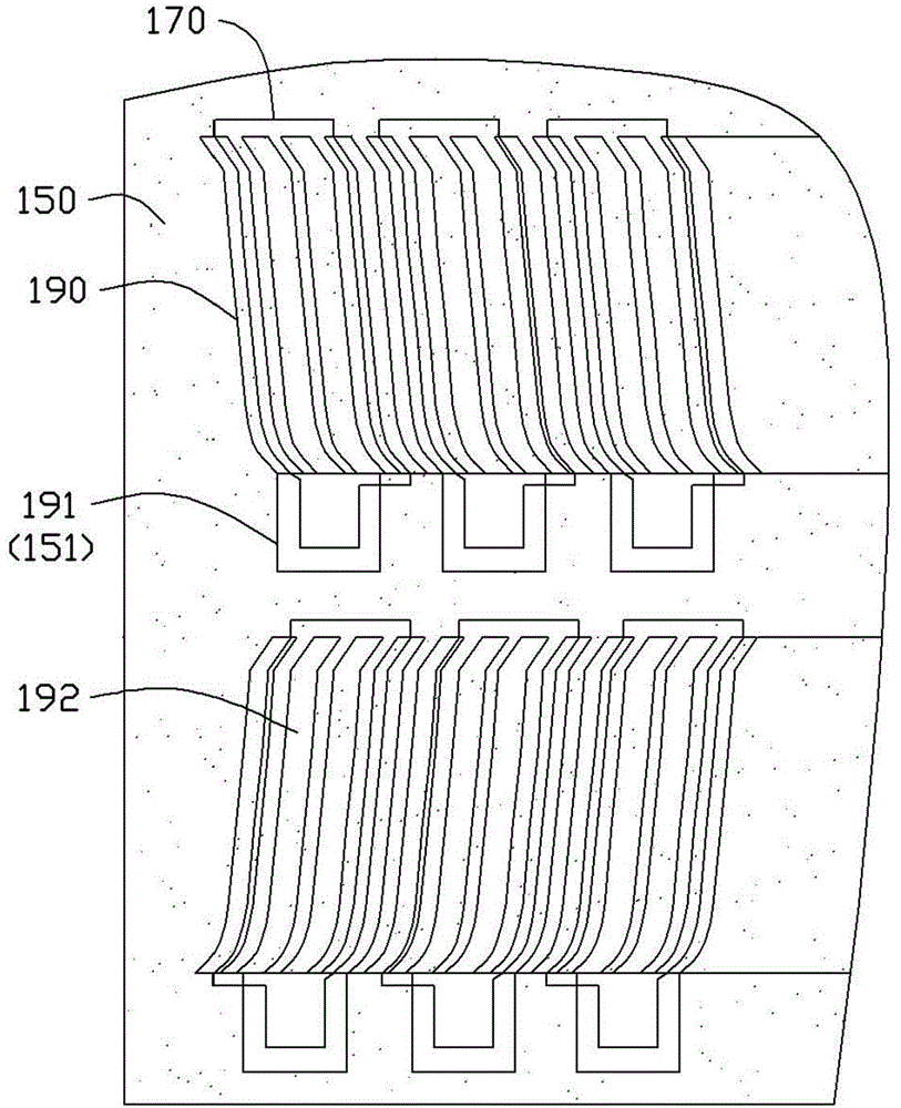
[0023] figure 1 It is a plan view of part of the liquid crystal display array substrate 100 according to the first embodiment of the present invention. In this embodiment, the liquid crystal display is an FFS type liquid crystal display. The array substrate 100 includes a plurality of scan lines GL arranged in parallel and a plurality of data lines DL arranged in parallel, and the scan lines GL and the data lines DL intersect to define a plurality of sub-pixels. Each sub-pixel includes a thin film transistor (TFT) 120 and a pixel electrode 170 . Wherein, the pixel electrode 170 is a plate-shaped electrode, respectively located in each sub-pixel, and electrically connected to the TFT 120 .

[0024] The array substrate 100 further includes a first common electrode 150 and a second common electrode 190 . In this embodim...


PUM


Abstract

An array substrate for a liquid crystal display device includes a first storage capacitor and a second storage capacitor for increased capacitance. The first storage capacitor is formed by a first common electrode and a pixel electrode. The second storage capacitor is formed by a second common electrode and the pixel electrode.

Description

technical field [0001] The invention relates to a liquid crystal display, in particular to an array substrate of a liquid crystal display. Background technique [0002] Currently, fringe field switching (FFS) type liquid crystal displays are very popular in the display market. In the fringe field electric field liquid crystal display, a pixel electrode and a common electrode are formed on an array substrate, and a voltage is applied between the pixel electrode and the common electrode to generate a fringe electric field to drive the liquid crystal in a plane substantially parallel to the array substrate. molecular. This liquid crystal display has the characteristics of wide viewing angle, low color shift and high aperture ratio. [0003] In recent years, the market has increasingly higher requirements for the resolution of displays. In order to increase the resolution, it is necessary to increase the pixel density of the array substrate of the liquid crystal display. How...

Claims


Application Information

Patent Timeline
Patent Type & Authority Applications(China)
IPC IPC(8): G02F1/1362G02F1/1343H01L27/02
CPCG02F1/136213G02F1/134309G02F2001/134372H01L27/1255H01L27/1244G02F1/134372G02F1/133555G02F1/134363G02F1/136227G02F1/133397
Inventor 蔡五柳高逸群林欣桦施博理李志隆
Owner HONG FU JIN PRECISION IND (SHENZHEN) CO LTD
Why Eureka
Try Eureka