Packaging structure and semiconductor process

A packaging structure and semiconductor technology, applied in semiconductor devices, semiconductor/solid-state device manufacturing, semiconductor/solid-state device components, etc., can solve the problems of increased material cost, reduced mechanical strength of sealant, and uneven distribution

Active Publication Date: 2015-03-25
ADVANCED SEMICON ENG INC
View PDF4 Cites 4 Cited by
  • Summary
  • Abstract
  • Description
  • Claims
  • Application Information

AI Technical Summary

Problems solved by technology

[0002] In the known packaging structure, several electrical connection elements are used to electrically connect the two substrates, and in order to maintain the distance between the two substrates, it is necessary to use high structural strength electrical connection elements (such as: copper) to support between the two substrates , resulting in an increase in material cost
Moreover, if the distance between the die on the lower substrate and the upper substrate is too small, the sealant is difficult to flow in, causing air or gaps in the space between the die on the lower substrate and the upper substrate, which may cause product defects, for example, because the sealant is between the die and the upper substrate. The uneven distribution between the substrates causes the mechanica...

Method used


Image

  • Packaging structure and semiconductor process
  • Packaging structure and semiconductor process
  • Packaging structure and semiconductor process

Examples


Embodiment Construction

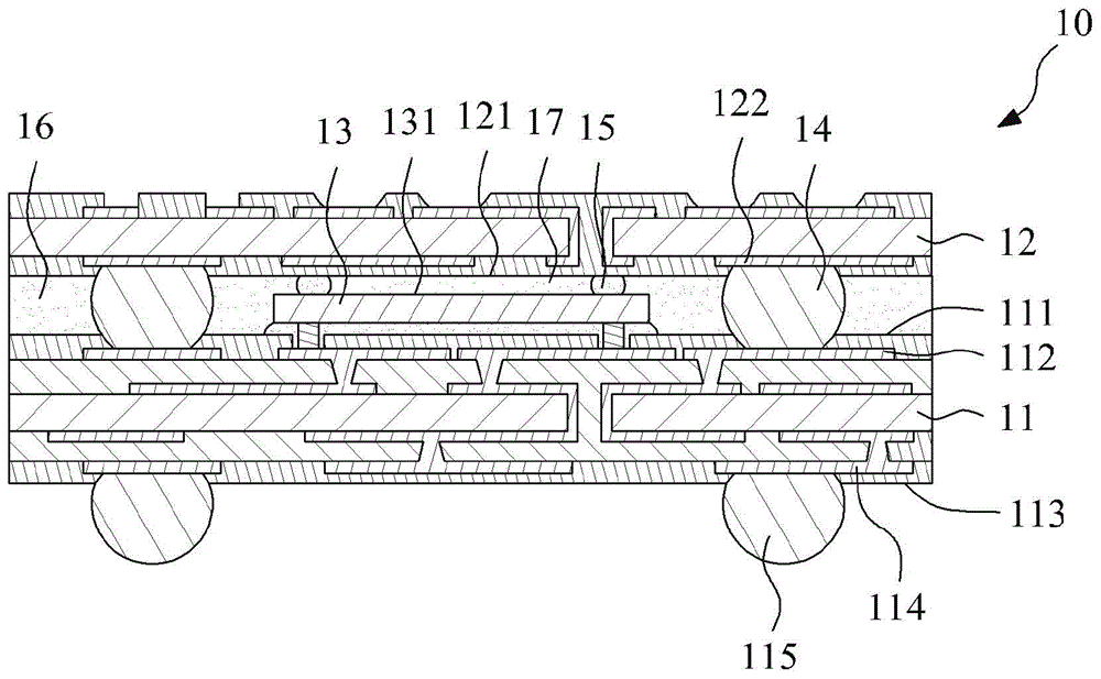
[0014] refer to figure 1 , shows a schematic cross-sectional view of an embodiment of the packaging structure of the present invention. The packaging structure 10 includes: a first substrate 11 , a second substrate 12 , a chip 13 , several electrical connection elements 14 , at least one spacer element 15 and a sealant 16 . The first substrate 11 has a first surface 111 and a plurality of first conductive contacts 112 , wherein the first conductive contacts 112 are exposed on the first surface 111 of the first substrate 11 . In one embodiment, the first substrate 11 further includes a first solder resist layer (not shown), the first surface 111 of the first substrate 11 is the surface of the first solder resist layer, and is exposed through the opening of the first solder resist layer The first conductive contact 112 . The first conductive contacts 112 can be conductive pads or conductive lines.

[0015] The second substrate 12 has a second surface 121 and a plurality of se...


PUM


Abstract

The invention relates to a packaging structure and a semiconductor process. The packaging structure comprises a first substrate, a second substrate, a grain, a plurality of electrical connection elements, at least one spacer element and a sealing compound. The grain is located between the first substrate and the second substrate; the at least one spacer element is arranged between the grain and the second substrate and is in contract with the grain and the second substrate. The electrical connection elements are electrically connected to the first substrate and the second substrate. The at least one spacer element is employed to support the second substrate, allowing a setting distance between the first substrate and the second substrate. The electrical connection elements do not require high intensity materials so as to reduce material cost. The at least one spacer element can control a distance and a space between the grain and the second substrate, allowing the sealing compound to smoothly flow into the space, avoiding generating air or gap in the space and increasing a product yield rate.

Description

technical field [0001] The invention relates to a packaging structure and a semiconductor process. Background technique [0002] In the known packaging structure, several electrical connection elements are used to electrically connect the two substrates, and in order to maintain the distance between the two substrates, it is necessary to use high structural strength electrical connection elements (such as: copper) to support between the two substrates , resulting in increased material costs. Moreover, if the distance between the die of the lower substrate and the upper substrate is too small, the sealant is difficult to flow in, causing air or gaps in the space between the die of the lower substrate and the upper substrate, which may cause product defects, for example, because the sealant is between the die and the upper substrate. The uneven distribution between the substrates results in a significant reduction in the mechanical strength of the sealant, reducing the reliab...

Claims


Application Information

Patent Timeline
IPC IPC(8): H01L21/603H01L23/488
CPCH01L2224/16225H01L2224/17H01L2224/1718H01L2224/32225H01L2224/73204H01L2924/00
Inventor 陈勇仁丁一权郑文吉
Owner ADVANCED SEMICON ENG INC
Why Eureka
Try Eureka