Ion to neutral control for wafer processing with dual plasma source reactor

A plasma and ion technology, which is applied in the field of control of the ratio of ions to neutral substances in an ion source reactor for processing wafers, and can solve problems such as being unsuitable for a second etching process and the like

Active Publication Date: 2015-03-25
LAM RES CORP
View PDF8 Cites 11 Cited by
  • Summary
  • Abstract
  • Description
  • Claims
  • Application Information

AI Technical Summary

Problems solved by technology

[0004] Because different processes are optimized in different ways, what is sui

Method used


Image

  • Ion to neutral control for wafer processing with dual plasma source reactor
  • Ion to neutral control for wafer processing with dual plasma source reactor
  • Ion to neutral control for wafer processing with dual plasma source reactor

Examples


Embodiment Construction

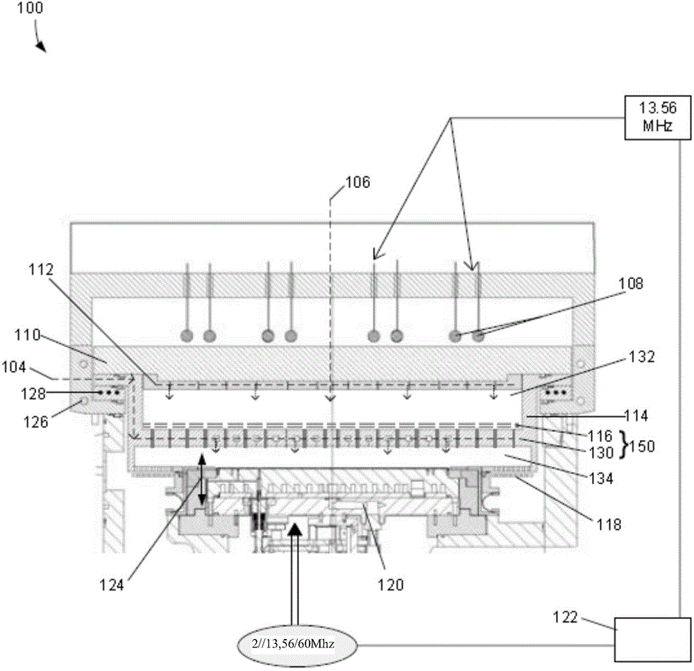
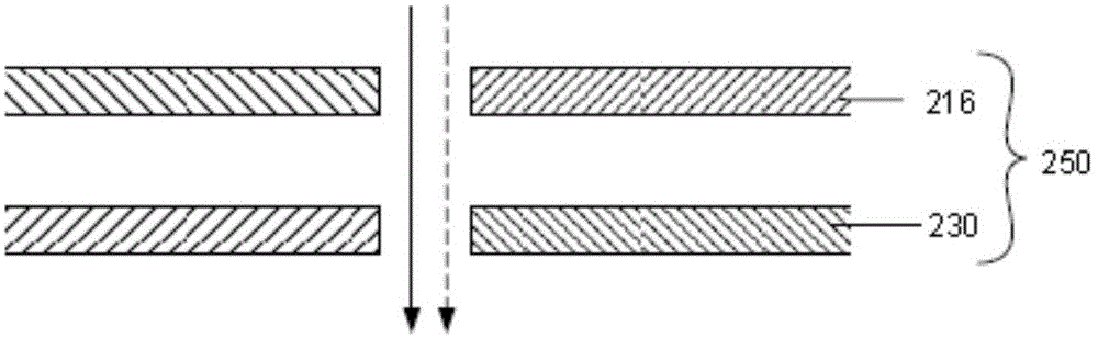
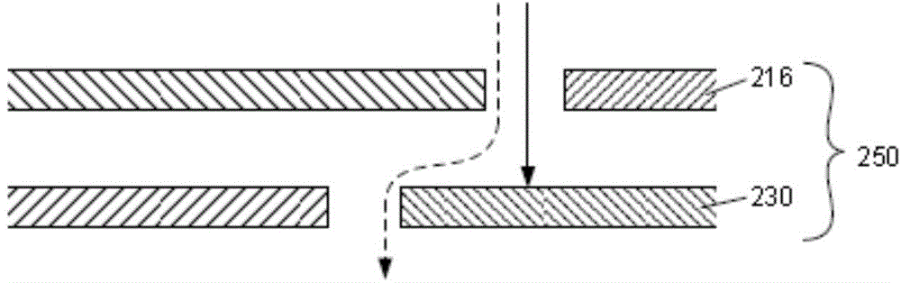
[0021]In this application, the terms "semiconductor wafer", "wafer", "substrate", "wafer substrate" and "partially fabricated integrated circuit" are used interchangeably. Those skilled in the art will appreciate that the term "partially fabricated integrated circuit" may refer to a silicon wafer during any of the many stages of fabrication of an integrated circuit on the silicon wafer. Wafers or substrates used in the semiconductor device industry typically have a diameter of 200 mm, or 300 mm, or 450 mm. Also, the terms "plate" and "grid" are used interchangeably. The following detailed description assumes that the invention is implemented on a wafer. However, the present invention is not limited thereto. Workpieces can be of various shapes, sizes, and materials. In addition to semiconductor wafers, other workpieces that may utilize the present invention include various items such as printed circuit boards and the like.

[0022] In the following description, numerous spe...


PUM


Abstract

The disclosed techniques relate to methods and apparatus for etching a substrate. A plate assembly divides a reaction chamber into a lower and upper sub-chamber. The plate assembly includes an upper and lower plate having apertures therethrough. When the apertures in the upper and lower plates are aligned, ions and neutral species may travel through the plate assembly into the lower sub-chamber. When the apertures are not aligned, ions are prevented from passing through the assembly while neutral species are much less affected. Thus, the ratio of ion flux:neutral flux may be tuned by controlling the amount of area over which the apertures are aligned. In certain embodiments, one plate of the plate assembly is implemented as a series of concentric, independently movable injection control rings. Further, in some embodiments, the upper sub-chamber is implemented as a series of concentric plasma zones separated by walls of insulating material.

Description

technical field [0001] The present invention generally relates to the field of semiconductor manufacturing, and more particularly to the control of the ratio of ions to neutral species in a dual plasma source reactor for processing wafers. Background technique [0002] One operation that is frequently used in semiconductor manufacturing is the etching operation. In an etching operation, one or more materials are partially or completely removed from a partially fabricated integrated circuit. Plasma etching is often employed, especially where the geometries involved are small, employ high aspect ratios, or require delicate pattern transfer. Typically, plasmas contain electrons, ions and free radicals. Free radicals and ions interact with the substrate to etch features, surfaces and materials on the substrate. [0003] As device dimensions shrink, plasma etch processes need to become increasingly precise and uniform in order to produce high-quality products. One driver for ...

Claims


Application Information

Patent Timeline
IPC IPC(8): H01L21/67H01L21/02
CPCH01L21/0274H01L21/0276H01L21/67359H01L2221/67H01J37/32357H01J37/32422H01J2237/334H01L21/3065H01L21/67069
Inventor 拉金德尔·迪恩赛南尚基阿列克谢·马拉赫塔诺夫埃里克·A·赫德森
Owner LAM RES CORP
Why Eureka
Try Eureka