Printed wiring board containing gold at different thicknesses and manufacturing method thereof

A printed circuit board, thin gold technology, applied in the direction of conductive pattern formation, etc., can solve the problems that the wire cannot be etched, the anti-plating dry film cannot resist the attack of gold-plating solution, etc., and achieve the effect of high mass production efficiency

Inactive Publication Date: 2015-03-25
GCI SCI & TECH
View PDF11 Cites 4 Cited by
  • Summary
  • Abstract
  • Description
  • Claims
  • Application Information

AI Technical Summary

Problems solved by technology

This method is only suitable for the production of printed circuit boards with low gold thickness. When the gold thickness is above 1.3 μm, the anti-plating dry film cannot resist the attack of gold plating solution, and the printed board will appear bleed-through, which will cause the wires to be unable to be etched away.

Method used


Image

  • Printed wiring board containing gold at different thicknesses and manufacturing method thereof
  • Printed wiring board containing gold at different thicknesses and manufacturing method thereof
  • Printed wiring board containing gold at different thicknesses and manufacturing method thereof

Examples


Embodiment Construction

[0037] The present application will be further elaborated below through specific examples.

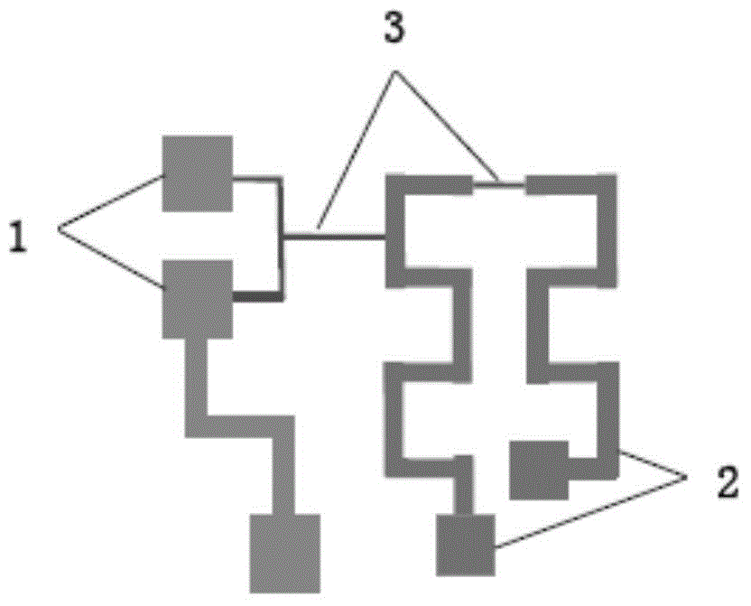
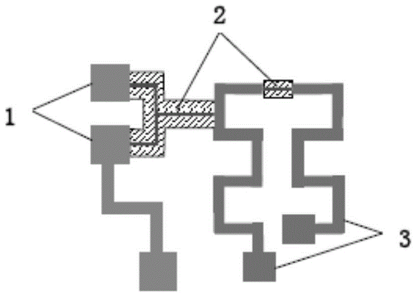
[0038] In this embodiment, a method for preparing a printed circuit board containing multiple gold thicknesses, the outer surface of the printed circuit board includes a thin gold region (thickness is 1.0 μm) and a thick gold region (thickness is 3.0 μm) , the line density is: 0.1mm≤line width≤0.5mm, 0.1mm≤pitch≤0.5mm; the preparation method includes the following steps:

[0039] (1) The first graphics transfer: make the required thin gold area and thick gold area and gold-plated wires on the outer surface of the printed circuit board, such as figure 1 As shown, 1 is a thin gold area, 2 is a thick gold area, and 3 is a gold-plated wire;

[0040] (2) Wet film printing: The printed circuit board obtained in step (1) is subjected to wet film printing and developing operations to expose thin gold areas and thick gold areas, such as figure 2 shown;

[0041] (3) gold plating for the firs...


PUM


Abstract

The invention discloses a printed wiring board containing gold at different thicknesses and a manufacturing method of the printed wiring board. An outer layer plate surface of the printed wiring board comprises a thin gold area and a thick gold area. The manufacturing method includes the following steps of pattern transferring for the first time, wet film printing, gold plating for the first time, pattern transferring for the second time, gold plating for the second time, film removing, pattern transferring for the third time and etching. According to the manufacturing method, manual wire cutting is not needed, and the efficiency of volume production is high; the requirement for machining with different gold thicknesses is satisfied; machining of the printed wiring board containing gold at two or more different thicknesses is achieved in the manner of protecting wires through wet films and protecting the thin gold area through dry films.

Description

technical field [0001] The invention relates to the technical field of printed circuit boards, in particular to a printed circuit board containing multiple gold thicknesses and a preparation method thereof. Background technique [0002] Under the trend of multi-functional and complex electronic products, all high-tech value-added electronic product designs are pursuing the characteristics of low power consumption, low electromagnetic radiation, high reliability, miniaturization, and light weight, which promotes the unprecedented development of printed circuit boards. The high-density state of the circuit board is getting denser and denser. At the same time, due to requirements such as cost reduction, more and more circuit board designs have put forward diversified requirements for the surface treatment of circuit boards according to the needs of use, gradually changing the traditional single surface treatment requirements. [0003] The diversified requirements for surface t...

Claims


Application Information

Patent Timeline
Patent Type & Authority Applications(China)
IPC IPC(8): H05K3/10
Inventor 陈亮白建国张峰关志锋
Owner GCI SCI & TECH
Why Eureka
Try Eureka