Through hole/contact hole for semiconductor

A contact hole and semiconductor technology, which is applied in the direction of semiconductor devices, semiconductor/solid-state device parts, electric solid-state devices, etc., can solve the problems of inability to connect and cannot be carried out, and achieve the effect of easy realization, avoiding connection methods, and improving product performance

Active Publication Date: 2018-01-19
XI AN UNIIC SEMICON CO LTD
View PDF4 Cites 0 Cited by
  • Summary
  • Abstract
  • Description
  • Claims
  • Application Information

AI Technical Summary

Problems solved by technology

[0005] In order to solve the technical problem that some stages need to be connected, some stages cannot be connected, and some stages cannot be carried out in the existing layout design, the present invention provides a through hole / contact hole for semiconductor

Method used


Image

  • Through hole/contact hole for semiconductor
  • Through hole/contact hole for semiconductor
  • Through hole/contact hole for semiconductor

Examples


Embodiment Construction

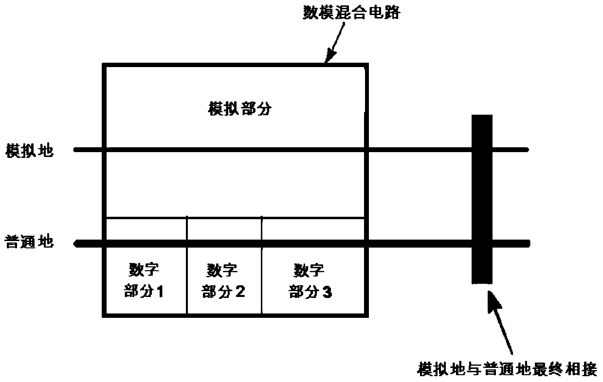
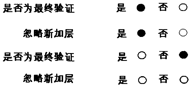
[0020] Such as figure 2 As shown, this via / contact hole adds a new layer (simulation layer) on the original basis. Analog layers exist in the layout design but not in the physical implementation. It surrounds the via hole / contact hole at a certain ratio. Such as figure 2 As shown, in practice, through the definition of the simulation layer and the setting of the verification rules, the simulation layer can be selected to be valid or invalid (ignored).

[0021] The analog layer is defined as the enclosing via hole. This layer is valid or invalid: that is, the analog layer is valid, and the via hole is invalid; the via / contact hole is regarded as only two layers of metal layers or one metal layer and one active area / polysilicon. If the analog layer is invalid, the via hole is valid, and the via hole / contact hole is a traditional via hole / contact hole at this time.

[0022] This way in practice, such special vias / contacts are placed at locations that would allow actual co...


PUM


Abstract

The present invention relates to a through hole / contact hole for a semiconductor, comprising a first contact layer 1, a via hole 3 and a second contact layer 2, the first contact layer 1 and the second contact layer 2 are connected through the via hole 3, and Including the simulation layer 4, the simulation layer surrounds the outside of the communication hole, through the definition of the simulation layer and the setting of the verification rules, the simulation layer can be selected to be valid or invalid. The invention solves the technical problem that some stages need to be connected, some stages cannot be connected, and some stages cannot be carried out in the existing layout design. The invention can reduce the realization difficulty caused by the gap between partial principle design and physical realization, reduce design time and error occurrence, improve design efficiency and product performance, and is simple and easy to implement.

Description

technical field [0001] The invention relates to a through hole / contact hole for semiconductors. Background technique [0002] In the semiconductor layout, the connection between the active area, polysilicon and metal layers needs to be realized through vias / contact holes. The connection between the active area, the polysilicon and the metal layer is called a contact hole. Connections between different metal layers are called vias. Generally, such a through hole / contact hole is composed of at least three parts (the contact hole in the active area will also have other components): the first contact layer 1, the through hole 3 and the second contact hole 2, the first contact layer is the active area. The source area, polysilicon or metal layer, and the second contact hole is the metal layer. [0003] In the previous layout design, the connection relationship of each physical layer is generally consistent with the design of the schematic diagram, and the connection sequence i...

Claims


Application Information

Patent Timeline
Patent Type & Authority Patents(China)
IPC IPC(8): H01L23/528
Inventor 李晓坤
Owner XI AN UNIIC SEMICON CO LTD
Why Eureka
Try Eureka