

A method and device for improving light-induced attenuation of crystalline silicon solar cell components
A technology of solar cells and light-induced attenuation, which is applied in the direction of electrical components, semiconductor devices, circuits, etc., can solve problems such as light-induced attenuation, achieve the effect of reducing and suppressing light-induced attenuation, simple method, and overcome cost investment
- Summary
- Abstract
- Description
- Claims
- Application Information
AI Technical Summary
Problems solved by technology
Method used
Image

Examples
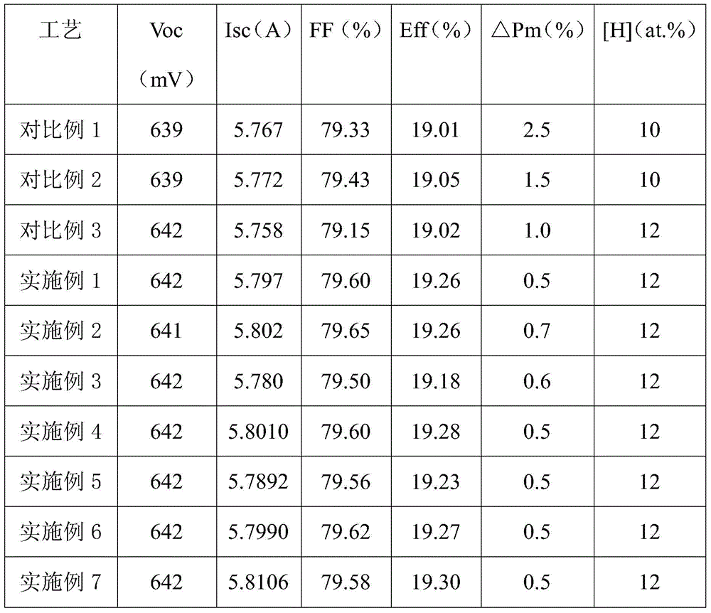
Embodiment 1
[0036] 1. Cell preparation:
[0037] (1) After the silicon wafers are sorted, perform rough polishing in an alkaline solution (NaOH or KOH solution) to remove impurities and damaged layers;
[0038] (2) Alkaline solution (NaOH or KOH solution) or acidic solution (HF+HNO 3) after velvet making, wash, dry, and the velvet surface size is within 5um;
[0039] (3) Perform high-temperature phosphorus diffusion in a diffusion furnace to form a pn junction, plasma etching to remove the edge junction and secondary cleaning to remove PSG, and the diffusion square resistance is 80-120ohm / squ;
[0040] (4) Depositing the front passivation layer / anti-reflection layer, this step is one of the key processes of the present invention. First, using PECVD (through SiH 4 and NH 3 ) Deposit a layer of SiNx on the emission region, the film thickness is 65nm, and the refractive index is 2.0-2.1; then, deposit SiOxNy film on the SiNx film (through SiH 4 , NH 3 and N 2 O), film thickness is 15n...
Embodiment 2
[0048] 1. Cell preparation:
[0049] PECVD (through SiH 4 and NH 3 ) Deposit a layer of SiNx on the emission region, the film thickness is 70nm, and the refractive index is 2.0-2.1; then, deposit SiOxNy film on the SiNx film (through SiH 4 , NH 3 and N 2 (2), the film thickness is 10nm, and the refractive index is 1.8-1.9; other processes are the same as in Embodiment 1.
[0050] 2. Component packaging: the same as in the first embodiment.
Embodiment 3
[0052] 1. Cell preparation:
[0053] PECVD (through SiH 4 and NH 3 ) Deposit a layer of SiNx on the emission region, the film thickness is 60nm, and the refractive index is 2.0-2.1; then, deposit SiOxNy film on the SiNx film (through SiH 4 , NH 3 and N 2 (2), the film thickness is 20nm, and the refractive index is 1.8-1.9; other processes are the same as in Embodiment 1.
[0054] 2. Component packaging: the same as in the first embodiment.
PUM
 Abstract
Description
Claims
Application Information