Organic electroluminescence device

An electroluminescent device and electroluminescent technology, which is applied in the direction of electro-solid devices, electrical components, semiconductor devices, etc., can solve the problems of complex preparation process of hole transport layer, achieve high product yield, reduce the number of alignments, improve The effect of process accuracy

Active Publication Date: 2015-04-08
KUNSHAN NEW FLAT PANEL DISPLAY TECH CENT +1
View PDF6 Cites 12 Cited by
  • Summary
  • Abstract
  • Description
  • Claims
  • Application Information

AI Technical Summary

Problems solved by technology

[0006] For this reason, the technical problem to be solved by the present invention lies in the problem in the prior art that has higher triplet energy level T1 and the complex preparation process of the mobility hole transport layer, and then provides an organic electroluminescence device, the hole The transport layer has a higher triplet energy level T1 and mobility, and the preparation process is simple, which in turn brings the beneficial effects of significantly reducing the power consumption of the device and greatly improving the efficiency

Method used


Image

  • Organic electroluminescence device
  • Organic electroluminescence device
  • Organic electroluminescence device

Examples


preparation example Construction

[0057] The preparation method of the organic electroluminescent device comprises the following steps:

[0058] In the preparation process of the organic electroluminescence device of the present invention, the preparation of the first electrode layer 1, the second electrode layer 8, the hole injection layer 2, the light-emitting unit layer and the second electrode layer 8 are all conventional techniques in the art. For the hole transport layer 3, the first hole transport material and the second hole transport material can be deposited by using an open mask.

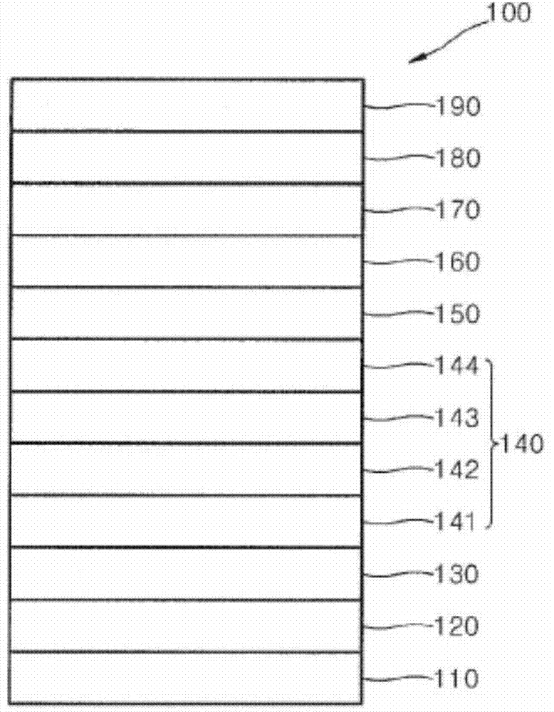
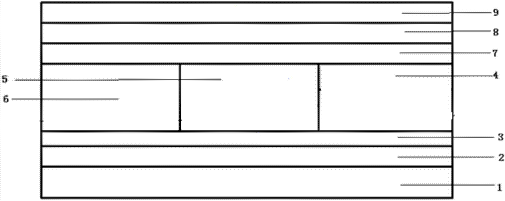
[0059] As a preferred embodiment, such as image 3 As shown, the hole transport layer includes a first hole transport layer 31 and a second hole transport layer 32 disposed on the first hole transport layer 31, and the first hole transport layer 31 is composed of Prepared from the first hole transport material, the second hole transport layer 32 is prepared from the first hole transport material and the second hole trans...

Embodiment 1

[0090] Example 1 Red light emitting device

[0091] The structure of device 1:

[0092] ITO(40nm) / HIL:3%HAT(170nm) / HTL-1:50%HTL-2(20nm) / CBP:5%Ir(piq) 3 (30nm) / Bphen(5nm) / Bphen:50%liq(30nm)Mg:Ag(2nm) / Ag(18nm) / Alq 3 (65nm)

[0093] Table 1 The performance test structure of the above three green light devices is as follows

[0094]

[0095] It can be found from Example 1 that the co-doping of the HTL layer improves the current efficiency, reduces the driving voltage, and prolongs the lifetime.

Embodiment 2

[0101] Example 2 Green light emitting device

[0102] The structure of device 2:

[0103] ITO(40nm) / HIL:3%HAT(140nm) / HTL-1:50%HTL-2(20nm) / CBP:5%Ir(ppy) 3 30nm) / Bphen(5nm) / Bphen:50%liq(30nm)Mg:Ag(2nm) / Ag(18nm) / Alq 3 (65nm)

[0104] According to the requirements of device performance, the proportion of HTL-1 can be adjusted from 10% to 90%.

[0105] Table 2 The performance test structure of the above three devices is as follows

[0106]

[0107] From Example 2, it can be found that the co-doping of the HTL layer improves the current efficiency, reduces the driving voltage, and prolongs the lifetime.

[0108] The structure of the red light-emitting device of Examples 3-10 is the same as that of Example 1, and the structure of the green light-emitting device of Examples 11-18 is the same as that of Example 2, and the composition of the red optical compensation layer and the green optical compensation layer is as follows :

[0109]

[0110] Example 15 ...


PUM


Abstract

The invention relates to an organic electroluminescence device which comprises a substrate, and a first electrode layer, a plurality of luminous units and a second electrode layer which are formed on the substrate in sequence, wherein the luminous units comprise a hole injection layer, a hole transmission layer, a luminous layer and an electronic transmission layer which are arranged on the first electrode layer in sequence; the hole transmission layer is prepared from a first hole transmission material and a second hole transmission material; the triplet energy level T1 of the first hole transmission material is greater than or equal to 2.48eV, and the HOMO energy level is smaller than or equal to -5.5eV; the HOMO energy level of the second hole transmission material is greater than -5.5eV; furthermore, the HOMO energy level difference between the first hole transmission material and the second hole transmission material is smaller than or equal to 0.2eV. The hole transmission layer is higher in triplet energy level T1 and migration rate, and the preparation technology is simple, so that the beneficial effects of obviously reducing the power consumption of the device and greatly improving the efficiency are achieved.

Description

technical field [0001] The invention relates to the technical field of organic electroluminescent devices, in particular to an organic electroluminescent device in which a hole transport layer material has relatively high triplet energy level T1 and mobility. Background technique [0002] The light-emitting layer of the organic electroluminescent device OLED is mainly made of all fluorescent materials, all phosphorescent materials or a mixture of fluorescent materials and phosphorescent materials. Because blue light, green light, and red light devices have different requirements for the hole transport layer HTL, especially green light and red light have high triplet energy level T1 for HTL materials, but HTL with high triplet energy level T1 Materials generally have low mobility, high driving voltage, and short life. Therefore, in order to meet the performance of red, green, and blue devices at the same time, HTL materials must have both high T1 and high mobility. At present...

Claims


Application Information

Patent Timeline
Patent Type & Authority Applications(China)
IPC IPC(8): H01L51/50H01L51/54
CPCH10K50/156
Inventor 李维维刘嵩
Owner KUNSHAN NEW FLAT PANEL DISPLAY TECH CENT
Why Eureka
Try Eureka