PMOS (p-channel metal oxide semiconductor) device and manufacturing method thereof

A manufacturing method and device technology, which is applied in semiconductor/solid-state device manufacturing, semiconductor devices, electrical components, etc., can solve the problems of PMOS performance improvement obstacles, achieve size reduction, improve performance, and increase the saturation current.

Inactive Publication Date: 2015-04-15
SEMICON MFG INT (SHANGHAI) CORP
View PDF6 Cites 4 Cited by
  • Summary
  • Abstract
  • Description
  • Claims
  • Application Information

AI Technical Summary

Problems solved by technology

[0006] However, the performance improvement of the existing PMOS is hindered after the size is reduced to a certain extent

Method used


Image

  • PMOS (p-channel metal oxide semiconductor) device and manufacturing method thereof
  • PMOS (p-channel metal oxide semiconductor) device and manufacturing method thereof
  • PMOS (p-channel metal oxide semiconductor) device and manufacturing method thereof

Examples


Embodiment Construction

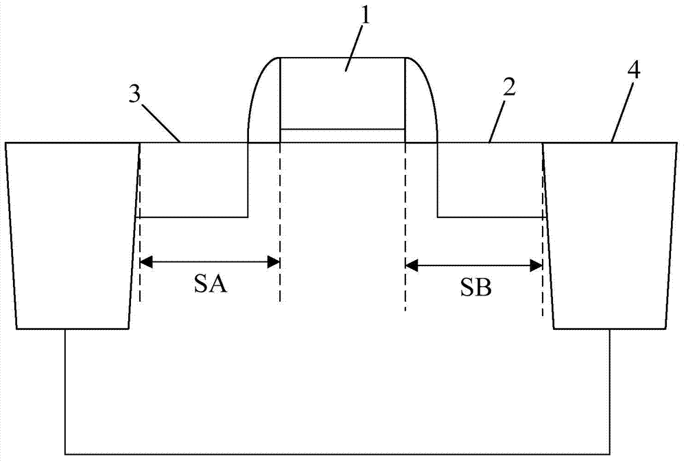
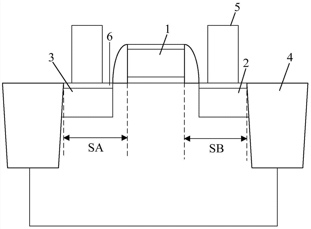
[0044] refer to figure 1 with figure 2 As shown, in the existing PMOS device, a conductive plug 5 is formed on the source region 3 and the drain region 2, and a contact layer 6 is also formed between the source region 3, the drain region 2 and the conductive plug 5 for Reduce contact resistance.

[0045] In order to prevent the deviation of the formation position of the conductive plug 5 , the conductive plug 5 is formed on the gate 1 (including the sidewall of the gate 1 ) or the isolation region 4 , thereby resulting in failure of the conductive plug 5 . The size of the existing source region 3 and drain region 2 is usually relatively large in the horizontal direction (such as figure 1 with figure 2 As shown, SA and SB represent the size of the source region 3 and the drain region 2 respectively, and SA and SB are usually 0.3 to 0.35 microns), so that even if there is a certain deviation in the position of the conductive plug 5 formed in the subsequent steps, the still...


PUM

PropertyMeasurementUnit
thicknessaaaaaaaaaa
thicknessaaaaaaaaaa

Abstract

A manufacturing method of a PMOS (p-channel metal oxide semiconductor) device includes providing a substrate, forming an isolation structure in the substrate, forming a grid and side walls above the substrate and forming a source area and a drain area in the substrate; forming a silicon layer on the surfaces of the source area, the drain area and the side walls; converting the silicon layer into a silicide contact layer; forming conductive plugs on the silicide contact layer. The invention further provides the PMOS device. The PMOS device comprises the substrate, the isolation structure, the source area, the drain area, the grid, the side walls, the silicide contact layer and the conductive plugs, wherein the isolation structure, the source area and the drain area are formed in the substrate, the grid and the side walls are arranged on the substrate between the source area and the drain area, the silicide contact layer is formed on the surfaces of the source area, the drain area and the side walls, and the conductive plugs are formed on the silicide contact layer. The PMOS device has the advantages that even if the conductive plugs deviate, the conductive plugs cannot be disconnected with the source area or the drain area, and the source area and the drain area are small enough, so that the performance of the PMOS device is improved.

Description

technical field [0001] The invention relates to the field of semiconductors, in particular to a PMOS device and a manufacturing method thereof. Background technique [0002] Complementary Metal Oxide Semiconductor (CMOS) is the basic unit in modern logic circuits, which includes PMOS and NMOS, and each PMOS or NMOS transistor is located on a doped well (Well), and the Both PMOS and NMOS are composed of a gate (Gate), a P-type or N-type source region (Source) region or a drain region (Drain) region located in the substrate on both sides of the gate, and a channel between the source region and the drain region ( Channel) constitutes. [0003] Since the size of the CMOS is getting smaller and smaller, correspondingly, the size of each part in the CMOS needs to be reduced proportionally. Among them, the size of the PMOS (Positive Channel Metal Oxide Semiconductor, PMOS) transistor will also be reduced accordingly, and the size of the source region (Source) and drain region (Dr...

Claims


Application Information

Patent Timeline
Patent Type & Authority Applications(China)
IPC IPC(8): H01L21/336
CPCH01L29/66477H01L29/78
Inventor 林爱梅吕瑞霖
Owner SEMICON MFG INT (SHANGHAI) CORP
Why Eureka
Try Eureka