Fingerprint sensor encapsulation method and structure

A fingerprint sensor and packaging structure technology, which is applied in the field of fingerprint sensor packaging methods and structures, can solve problems such as low reliability, complex fingerprint sensor packaging technology, and short-circuit risk, and achieve improved reliability, simple and reliable packaging structure, The effect of simplifying the manufacturing process

Active Publication Date: 2015-04-15
SKY CHIP INTERCONNECTION TECH CO LTD
View PDF7 Cites 18 Cited by
  • Summary
  • Abstract
  • Description
  • Claims
  • Application Information

AI Technical Summary

Problems solved by technology

[0005] The embodiment of the present invention provides a fingerprint sensor packaging method and structure to solve the technical problems of the existing fingerprint sensor packaging technology with complex process, short circuit risk and low reliability

Method used


Image

  • Fingerprint sensor encapsulation method and structure
  • Fingerprint sensor encapsulation method and structure
  • Fingerprint sensor encapsulation method and structure

Examples


Embodiment 1

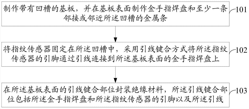
[0019] Please refer to figure 1 , an embodiment of the present invention provides a fingerprint sensor packaging method, the method comprising:

[0020] 101. Fabricate a substrate with a groove, and fabricate a gold finger pad and at least one metal strip adjacent to or adjacent to the groove on the surface of the substrate.

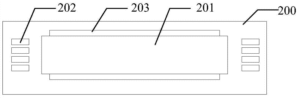
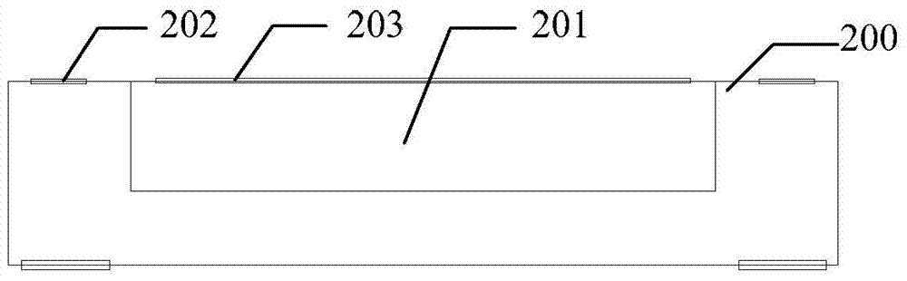
[0021] Such as Figure 2a with 2b As shown, a groove 201 is processed on the substrate 200 produced in this embodiment, and the groove 201 will be used to embed the fingerprint sensor in the future. The size of the groove matches the size of the fingerprint sensor, and the depth of the groove should be deeper than that of the fingerprint sensor. The thickness is slightly larger, for example, about 50 microns larger. The groove can be processed by means of controlled depth milling or laser etching. The position on the surface of the substrate 200 close to the groove 201 is pre-processed with gold finger pads 202 for connecting with pins on the fingerp...

Embodiment 2

[0035] Please refer to Figure 5a with 5b , an embodiment of the present invention provides a fingerprint sensor packaging structure, including:

[0036] A substrate 200 with a groove 201 and a fingerprint sensor 300 fixed in the groove 201, the surface of the substrate 200 has at least one metal strip 203 adjacent to or adjacent to the groove 201, the lead of the fingerprint sensor 300 The pins are connected to the gold finger pads 202 on the surface of the substrate 200 through wires 204, and the wire bonding parts on the surface of the substrate 200 are covered with insulating materials, and the wire bonding parts include the gold finger pads 202 and the The pins of the fingerprint sensor 300 and the leads 204 are described.

[0037] In one embodiment, the groove 201 is a rectangular groove, and two metal strips 203 are adjacent to or adjacent to two opposite side walls of the rectangular groove 201 and distributed on the surface of the substrate 200 .

[0038] Optionall...


PUM


Abstract

The invention discloses a fingerprint sensor encapsulation method. The fingerprint sensor encapsulation method includes the following steps that: a substrate with a groove is manufactured, and at least one metal bar which adjoins or is adjacent to the groove is manufactured on the surface of the substrate; a fingerprint sensor is fixed in the groove, and pins of the fingerprint sensor are connected onto gold finger pads on the surface of the substrate through leads based on lead bonding; lead bonding portions on the surface of the substrate are encapsulated with an insulation material, wherein the lead bonding portions include the gold finger pads, the pins of the fingerprint sensor and the leads. The embodiment of the invention also provides a corresponding fingerprint sensor encapsulation structure. According to the technical scheme of the invention, a metal frame is not required to be installed in a surface-mount manner, and therefore, production process is simplified, and the encapsulation structure is simpler and more reliable; and the gold finger pads and the metal bars are formed through etching when the substrate is machined, and therefore, risks of short-circuiting can be avoided, and reliability can be greatly improved.

Description

technical field [0001] The invention relates to the technical field of fingerprint sensors, in particular to a fingerprint sensor packaging method and structure. Background technique [0002] A fingerprint sensor refers to a device that can automatically collect fingerprints. Its type is generally a semiconductor fingerprint sensor. On the other side of the inductance, due to the unevenness of the finger plane, the actual distance between the convex point and the concave point touching the plate is different, and the resulting capacitance / inductance value is also different. According to this principle, the different values ​​collected are summarized. , which completes the collection of fingerprints. [0003] The fingerprint sensor package belongs to a special kind of package. The part of the fingerprint sensor used for contact with the finger needs to be exposed, while the other lead connection parts need to be sealed and protected. In order to eliminate the static electri...

Claims


Application Information

Patent Timeline
Patent Type & Authority Applications(China)
IPC IPC(8): H01L21/56H01L23/488G06K9/00
CPCH01L24/97H01L2224/32225H01L2224/45124H01L2224/45144H01L2224/45147H01L2224/48091H01L2224/73265H01L2924/00014
Inventor 李冠华江京丁鲲鹏鲍平华彭勤卫孔令文
Owner SKY CHIP INTERCONNECTION TECH CO LTD
Why Eureka
Try Eureka