Absorption circuit for absorbing spike voltage of two-transistor forward converter
A forward converter and absorption circuit technology, applied in the field of absorption circuits, can solve the problems of large energy loss, low energy efficiency, and large heat generation, and achieve the effects of suppressing voltage spikes, low heat generation, and avoiding large losses
- Summary
- Abstract
- Description
- Claims
- Application Information
AI Technical Summary
Problems solved by technology
Method used
Image
Examples
Embodiment Construction
[0018] The principles and features of the present invention are described below in conjunction with the accompanying drawings, and the examples given are only used to explain the present invention, and are not intended to limit the scope of the present invention.
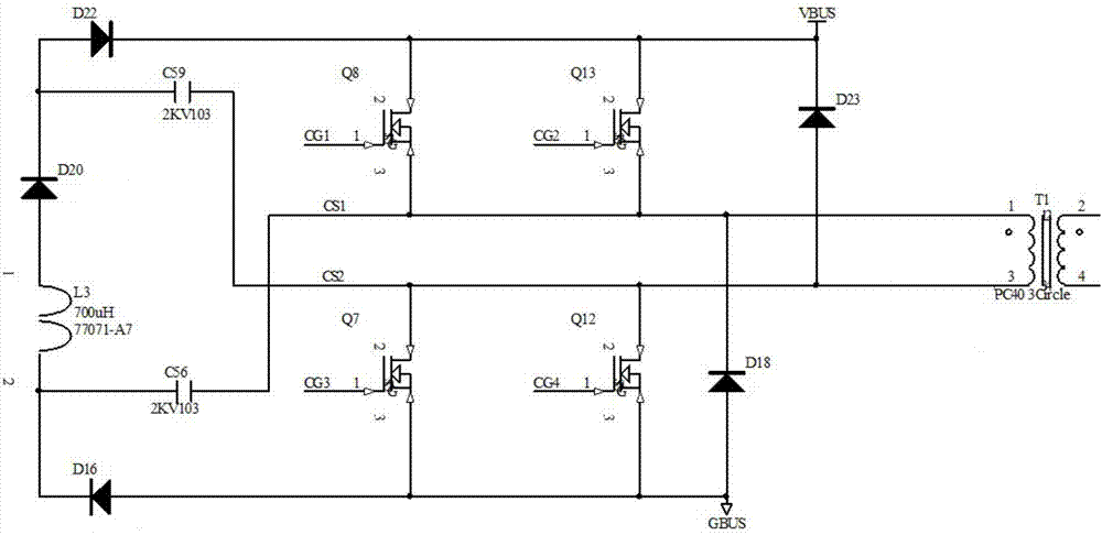
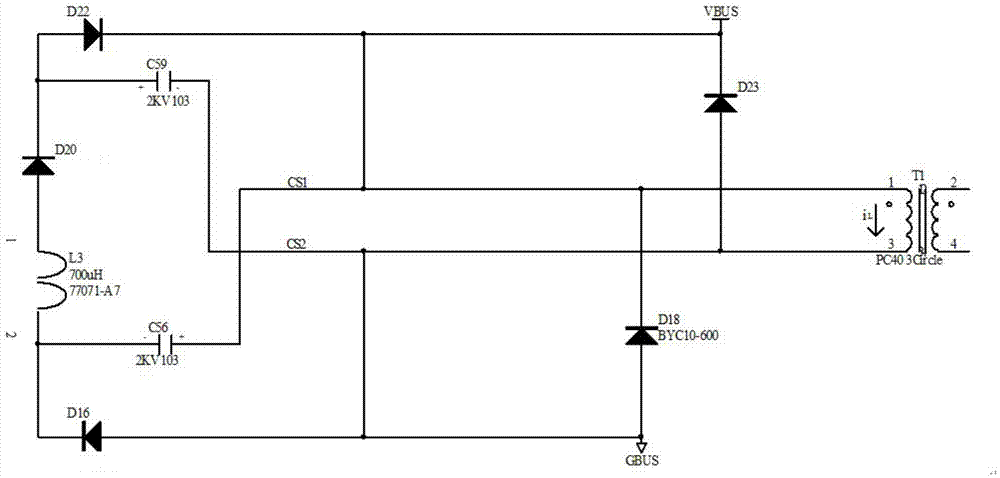
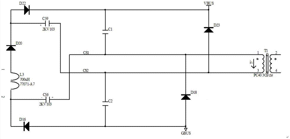
[0019] This embodiment is a snubber circuit for absorbing the peak voltage of a dual-transistor forward converter. This snubber circuit is a passive and lossless circuit, including two switch tubes Q8 and Q7. In other embodiments, Q8 may also be included. , Q7, Q13, Q12 four switch tubes, such as figure 1 shown. In the figure, C59 and C56 are the snubber capacitors of Q8 and Q13, Q7 and Q12 respectively, D16 and D22 are respectively unidirectional conductive snubber diodes, which provide a unidirectional conductive circuit during the action of the snubber circuit when the switching tube is disconnected; L3 uses The sendust magnetic ring provides a reset circuit for the absorption circuit; D18 and D23 are the clampi...
PUM
 Abstract
Description
Claims
Application Information


