Stable doping method for graphene

A graphene and graphene surface technology, which is applied in the field of stably improving the electrical properties of graphene films, can solve problems affecting the stability of square resistance, reduction of doping effects, disappearance, etc., to achieve improved time stability, quality, and stability sexual effect

Active Publication Date: 2015-04-22
CHONGQING GRAPHENE TECH +1
View PDF8 Cites 10 Cited by
  • Summary
  • Abstract
  • Description
  • Claims
  • Application Information

AI Technical Summary

Problems solved by technology

The existing doping technology is generally to do doping modification on the surface of graphene. The dopant attached to the surface of graphene is easily affected by various impurities in the air. As time goes by, the doping effect decreases or even disappears, thus affecting The stability of square resistance limits the application of graphene films in industrial fields such as display technology that require high square resistance of transparent conductive films

Method used


Image

  • Stable doping method for graphene
  • Stable doping method for graphene
  • Stable doping method for graphene

Examples


Embodiment 1

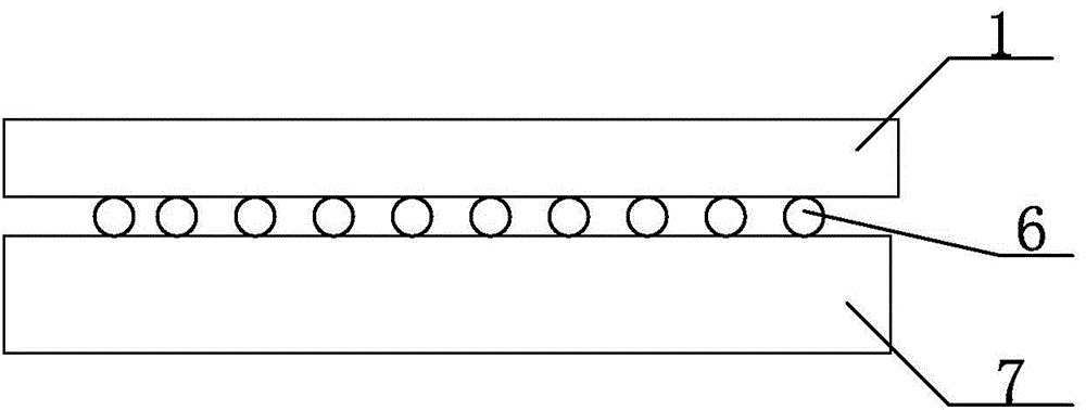
[0043] Such as figure 1 The graphene stable doping structure of the shown dopant between the substrate and graphene, the process is as follows Figure 8 As shown, the specific steps are as follows:

[0044] 1.1) Graphene is grown on the copper foil by CVD, and then the temporary substrate is pasted on the graphene;

[0045] 1.2) Put the copper foil into the etching solution, etch the copper foil to obtain a temporary substrate / graphene sample, and then put the graphene surface of the sample into the doping solution for doping, Then bond one side of the doped graphene to the substrate, then remove the temporary substrate to obtain a sample sheet with a dopant on the graphene surface, and finally obtain the substrate, dopant and graphene from bottom to top. sequential dailies; or,

[0046] Put the copper foil / graphene into the mixed solution composed of etching solution and doping solution, etch and dope at the same time, then attach the doped graphene side to the substrate, ...

Embodiment 2

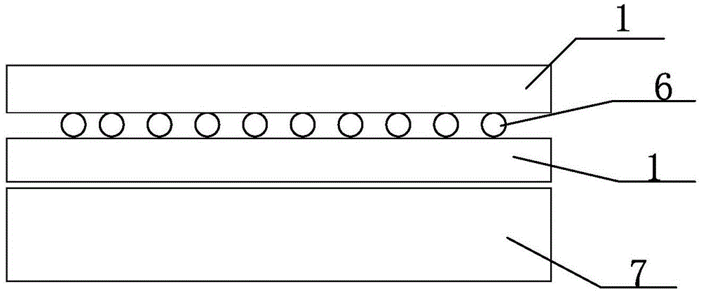
[0048] Such as figure 2 The stable doping structure of the shown dopant between the graphene and the graphene layer, the process is as follows Figure 9 As shown, the specific steps are as follows:

[0049] Step 1) Graphene is grown on the copper foil by CVD, and then the temporary substrate is pasted on the graphene;

[0050] Step 2) Put the copper foil into an etching solution, etch, wash and dry the copper foil to obtain a temporary substrate / graphene layer sample, and connect the graphene side of the sample to the substrate Bonding, and then remove the temporary substrate, then put the graphene surface into the doping solution for doping, after washing and drying, a sample with dopant on the graphene surface is obtained;

[0051] Step 3) the sample sheet that is provided with dopant on the graphene surface is pasted on the sample sheet of another temporary substrate / graphene layer, and then removes described temporary substrate, obtains successively from bottom to top as ...

Embodiment 3

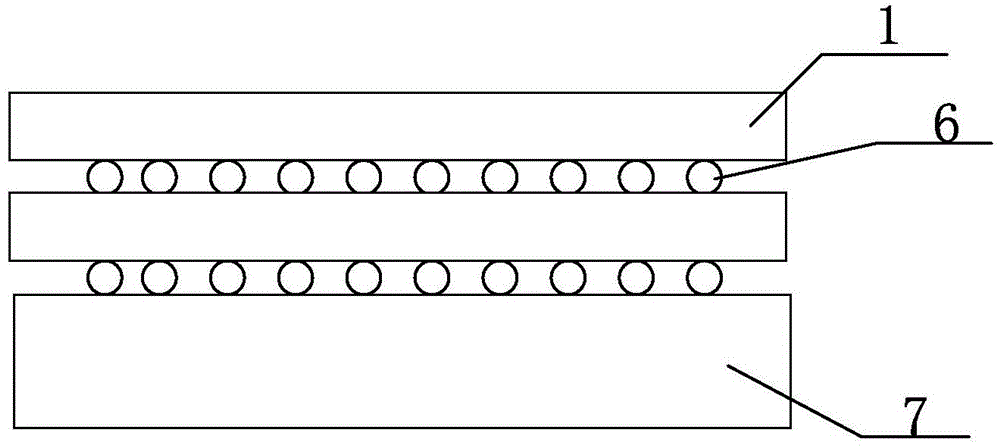
[0053] Such as image 3 The double-layer stable doping structure of the shown dopant between the substrate and graphene, graphene and graphene, the process is as follows Figure 8 , Figure 9 As shown, the specific steps are as follows:

[0054] The step of wrapping dopant reagent molecules between graphene and graphene is specifically as follows:

[0055] Step 1) Graphene is grown on the copper foil by CVD, and then the temporary substrate is pasted on the graphene;

[0056] Step 2) Put the copper foil into an etching solution, etch, wash and dry the copper foil to obtain a temporary substrate / graphene layer sample, and connect the graphene side of the sample to the substrate Bonding, and then remove the temporary substrate, then put the graphene surface into the doping solution for doping, after washing and drying, a sample with dopant on the graphene surface is obtained;

[0057] Step 3) the sample sheet that is provided with dopant on the graphene surface is pasted on ...


PUM

PropertyMeasurementUnit
concentrationaaaaaaaaaa
thicknessaaaaaaaaaa

Abstract

The invention relates to a stable doping method for graphene. The stable doping method for the graphene comprises the step of wrapping the doping agent between two pieces of graphene and/or wrapping a doping agent between a substrate and the graphene, wherein no clinical substrate is used in the step of wrapping the doping agent between the substrate and the graphene. The stable doping method for the graphene has the advantages that a stable doping effect is realized, a doping agent molecule is overlaid between a graphene layer and a substrate layer, the direct contact between the air and the doping agent molecule is avoided, and the original doping state of the doping agent molecule on the surface of the graphene is maintained for a long time, so that the long-term stable doping effect can be guaranteed.

Description

technical field [0001] The invention relates to a stable doping method of graphene, in particular to a method for stably improving the electrical properties of a graphene film, and belongs to the field of graphene film processing methods. Background technique [0002] graphene is sp 2 A two-dimensional material in which hybridized carbon atoms are arranged in a hexagonal lattice. The unique two-dimensional crystal structure endows graphene with unique properties. The thickness of single-layer graphene is 0.34nm, the light absorption is only 2.3% in a wide band, and the intrinsic carrier mobility is as high as 2.0×10 5 cm 2 ·V -1 ·s -1 , which makes graphene essentially have high transmittance and good conductivity at the same time, and can be used as a transparent conductive material. [0003] At present, the preparation methods of graphene films mainly include chemical vapor deposition method. Generally, the graphene prepared by this method cannot be used directly on ...

Claims


Application Information

Patent Timeline
Patent Type & Authority Applications(China)
IPC IPC(8): C01B31/04
Inventor 黄德萍姜浩朱鹏李占成张永娜高翾史浩飞
Owner CHONGQING GRAPHENE TECH
Why Eureka
Try Eureka