Graphene sensor, manufacturing method thereof and touch display device

一种石墨烯、石墨烯层的技术,应用在照相制版工艺曝光装置、仪器、感光材料加工等方向,能够解决导电性变差等问题,达到提高良率、减少数量、降低制作成本的效果

Inactive Publication Date: 2015-04-22
BOE TECH GRP CO LTD
View PDF3 Cites 9 Cited by
  • Summary
  • Abstract
  • Description
  • Claims
  • Application Information

AI Technical Summary

Problems solved by technology

[0004] Aiming at the defects of the prior art, the present invention provides a graphene touch sensor and its manufacturing method and a touch display device, which avoids the conductivity change caused by the contact of the alkaline developer and the alkaline stripper in the photolithography process with the graphene film. Poor problem, improve yield and reduce cost

Method used


Image

  • Graphene sensor, manufacturing method thereof and touch display device
  • Graphene sensor, manufacturing method thereof and touch display device
  • Graphene sensor, manufacturing method thereof and touch display device

Examples


Embodiment 1

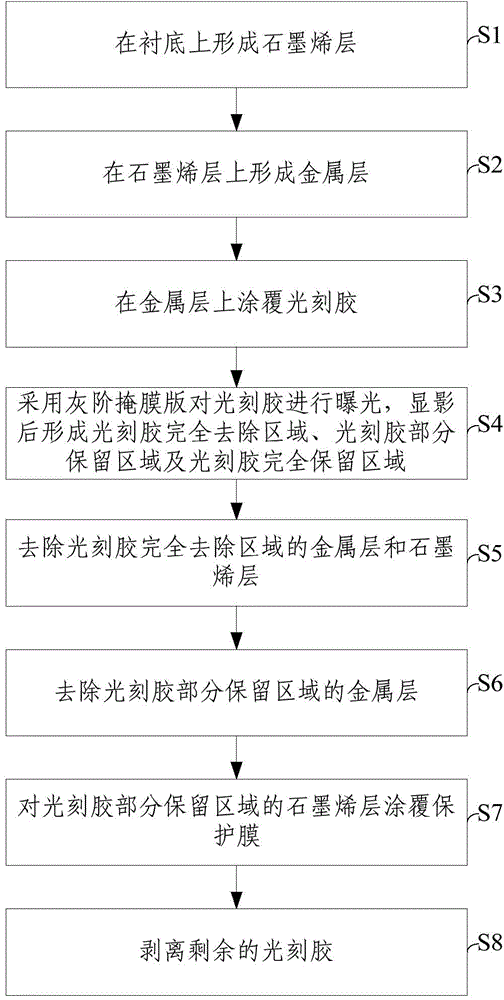
[0056] In order to illustrate the technical solution of the present invention more clearly, Embodiment 1 is illustrated below in conjunction with the schematic cross-sectional view of the device structure formed in each step, as Figure 9 As shown, the manufacturing method of this embodiment may specifically include the following steps:

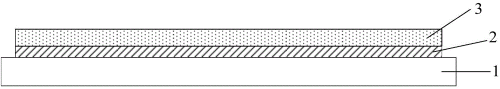
[0057] S10: forming a graphene layer 2 on the substrate 1, and depositing a sputtered metal film on the graphene layer 2 to form a metal layer 3, such as figure 2 shown;

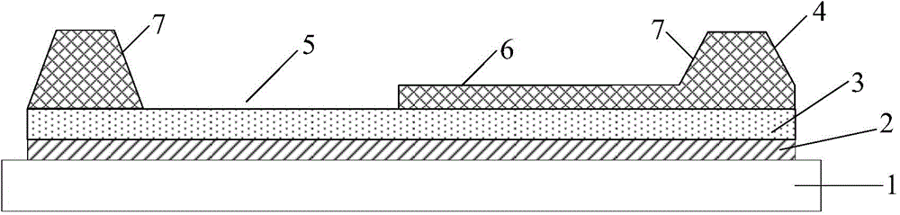
[0058] S20: Coating photoresist 4 on the metal layer 3, exposing and developing the photoresist 4 with a gray scale mask to form photoresist completely removed region 5, photoresist partially retained region 6 and photoresist Glue completely preserves region 7, as image 3 shown;

[0059] S30: using an acidic solution to wet etch the photoresist to completely remove the metal layer 3 in the region 5, such as Figure 4 shown;

[0060] S40: dry etching the photoresist t...


PUM

PropertyMeasurementUnit
visible light transmittanceaaaaaaaaaa
tensile strengthaaaaaaaaaa

Abstract

The invention provides a manufacturing method for a graphene touch sensor. The manufacturing method includes the steps that a graphene layer is formed on a substrate; a metal layer is formed on the graphene layer; the metal layer is coated with photoresist; the photoresist is exposed by adopting a gray scale mask plate, and a complete photoresist removing region, a partial photoresist reserving region and a complete photoresist reserving region are formed after development is carried out; the portions, in the complete photoresist removing region, of the metal layer and the graphene layer are removed; the portion, in the partial photoresist reserving region, of the metal layer is removed; the portion, in the partial photoresist reserving region, of the graphene layer is coated with a protective film; the remaining photoresist is peeled off. The invention further provides a graphene sensor obtained by adopting the manufacturing method and a touch display device comprising the graphene sensor. The problem that the electrical conductivity of a graphene thin film becomes poor as an alkaline developing solution and an alkaline peeling solution make contact with the graphene thin film in the photolithography technology is solved, the yield is increased, and cost is reduced.

Description

technical field [0001] The invention relates to the technical field of touch screens, in particular to a graphene sensor, a manufacturing method thereof, and a touch display device. Background technique [0002] Graphene is a carbon atom with sp 2 Hybrid orbitals (one s orbital and two p orbital hybrids) form a hexagonal flat film with a honeycomb lattice, a two-dimensional material with a thickness of only one carbon atom, and a thickness of only 0.335nm. The light transmittance of single-layer graphene is 97.7%, with high light transmittance, no reflection, and ultra-high carrier mobility (2*10 5 cm 2 / Vsec), high flexibility, high mechanical strength (tensile strength 10-20GPa), high chemical stability, high thermal conductivity and other excellent properties. As a transparent conductive film, graphene can be used to make ultra-thin, ultra-light, high-transmittance, flexible touch screens. [0003] The development trend of touch screen is large size, narrow frame, ult...

Claims


Application Information

Patent Timeline
Patent Type & Authority Applications(China)
IPC IPC(8): G06F3/041
CPCG06F3/041G06F2203/04103G03F7/16G03F7/20G03F7/32G03F7/422H05K1/092
Inventor 邸云萍刘震
Owner BOE TECH GRP CO LTD
Why Eureka
Try Eureka