

Preparation method of storage unit gate of flash memory
A technology for memory cells and gates, which is applied in electrical components, semiconductor/solid-state device manufacturing, electrical solid-state devices, etc. problems such as loss of floating gate layer, etc., to achieve the effect of good etching and forming effect, saving production time, improving performance and reliability
- Summary
- Abstract
- Description
- Claims
- Application Information
AI Technical Summary
Problems solved by technology
Method used
Image


Examples
preparation example Construction
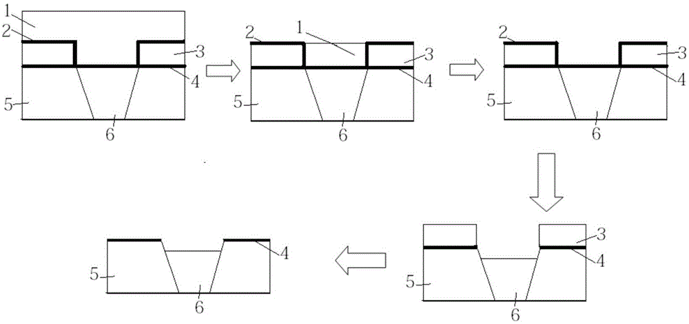
[0033] The invention provides a method for preparing a gate of a storage unit of a flash memory, which can be applied to a process with a technology node of 45 / 40nm and can be applied to a Flash technology platform.
[0034] The core idea of the present invention is that by synchronously etching the inter-gate dielectric layer and the floating gate structure, the etching method can effectively reduce the loss of shallow trench isolation regions, benefit subsequent processes, and ultimately improve the performance of semiconductor devices and reliability. Simultaneously using the method, the process is simple, the production time is saved, and the production efficiency is improved.
[0035] The method of the present invention will be described in detail below in conjunction with the accompanying drawings.
PUM
 Abstract
Description
Claims
Application Information