Nanoparticle detection system and screening analysis method
A nanoparticle, detection system technology, applied in particle and sedimentation analysis, particle size analysis, measuring devices, etc., can solve the problems of inability to obtain, quantify, and high cost
- Summary
- Abstract
- Description
- Claims
- Application Information
AI Technical Summary
Problems solved by technology
Method used
Image
Examples
Embodiment 1
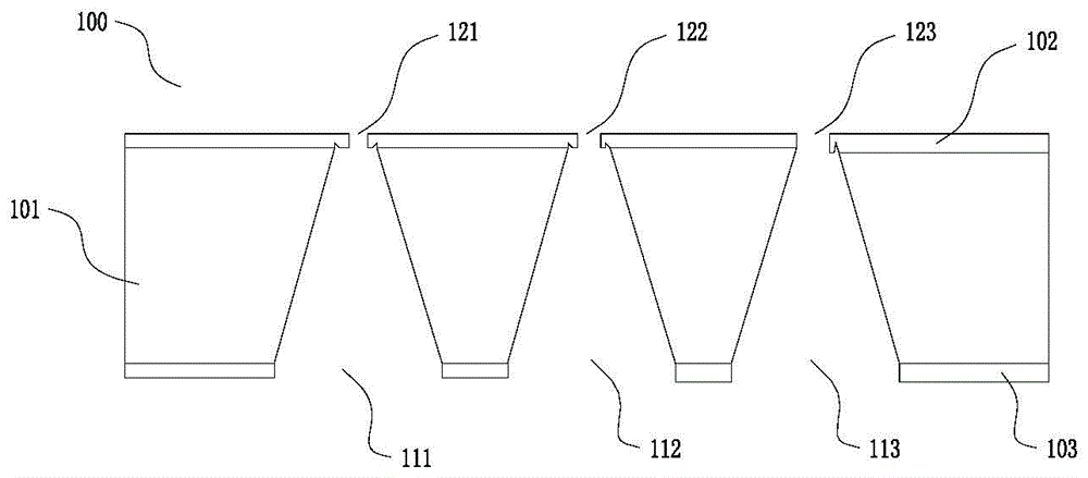
[0044] According to attached figure 1 Shown is the screening layer 100 of this embodiment, and the screening layer 100 includes a substrate 101, and the upper and lower surfaces of the substrate 101 are provided with electrically insulating thin film layers 102, 103. An array of screening channels is provided on the screening layer 100 , and the minimum diameter of each screening channel in the array is different. The screening channels 111 , 112 , 113 extend from the first surface to the second surface of the substrate 101 and thus penetrate the substrate 101 . Openings corresponding to these through holes are formed on the electrical insulating films 102 and 103 . exist figure 1 In the example of , these screening channels 111, 112, 113 are shown as shapes that gradually increase from top to bottom. Such through holes can be obtained by etching the substrate with the open electrical insulating film as a mask, as follows.
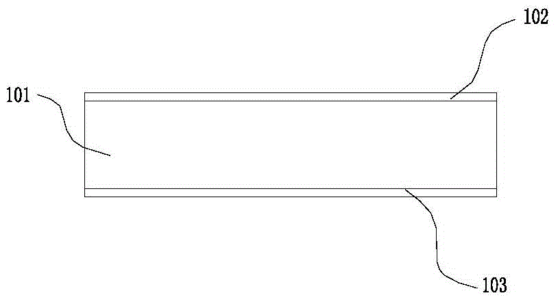
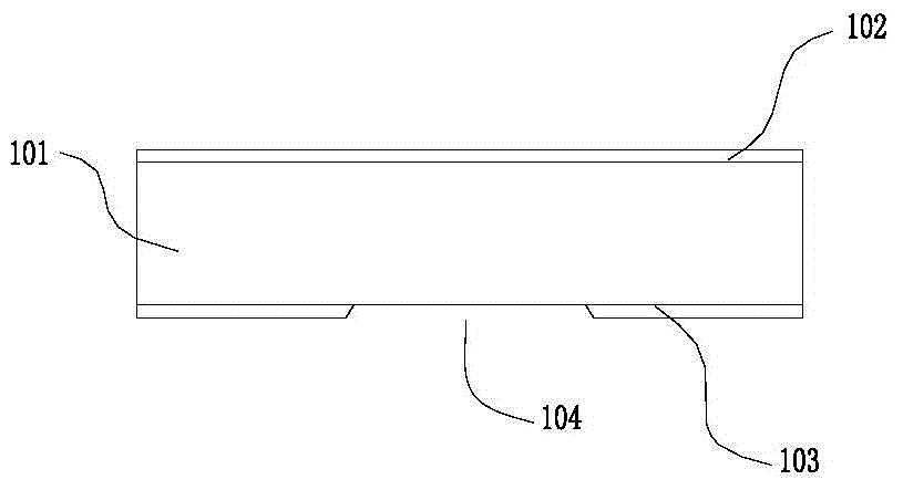
[0045] According to attached Figure 2a As show...
Embodiment 2
[0073] Referring to Embodiment 1, this embodiment adopts a structure in which the screening channel extends along the substrate plane, and the others are the same as Embodiment 1.
[0074]The screening channel extends along the plane of the substrate, thus taking the form of a trench on the substrate. Particle screening channels can communicate with other channels that guide ions. For example, particles may be directed from an entry channel to a particle screening channel, through the particle aperture through the particle screening channel, and then directed to exit the channel.
[0075] Figure 5 is a cross-sectional view schematically showing a particle screening channel array formed on a substrate according to another embodiment of the present disclosure.
[0076] Such as Figure 5 As shown, the array of particle screening channels includes a substrate 500, such as a silicon wafer. On the substrate 500, one or more (two are shown in the figure) particle screening chann...
PUM
 Abstract
Description
Claims
Application Information


