FPGA program multi-image loading method based on ARM

A multi-mirror and program technology, applied in the direction of program loading/starting, program control devices, etc., can solve the problem of slow switching speed, achieve the effect of fast switching speed and improve product production efficiency

Active Publication Date: 2015-04-29
WUHAN JINGCE ELECTRONICS GRP CO LTD
View PDF6 Cites 12 Cited by
  • Summary
  • Abstract
  • Description
  • Claims
  • Application Information

AI Technical Summary

Problems solved by technology

This method realizes the method of loading and running the FPGA program automatically. Although the running speed is improved and the original function will not b...

Method used


Image

  • FPGA program multi-image loading method based on ARM
  • FPGA program multi-image loading method based on ARM

Examples


Embodiment Construction

[0018] Below in conjunction with accompanying drawing and specific embodiment the present invention is described in further detail:

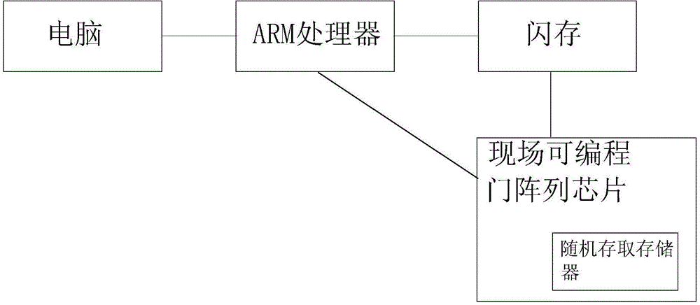
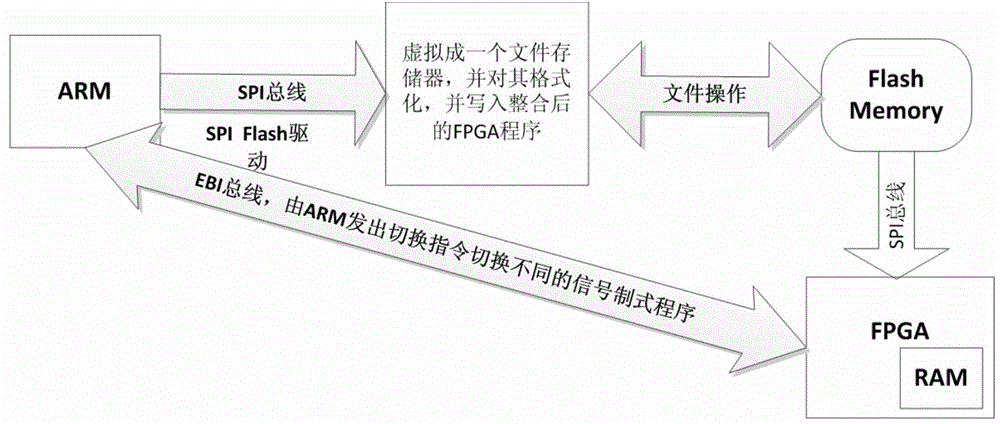
[0019] The hardware environment of the FPGA program multi-image loading method based on ARM of the present invention, such as figure 1 Described it comprises: computer, ARM processor, flash memory, field programmable gate array chip and the random access memory of field programmable gate array chip, described computer is connected ARM processor, and ARM processor passes serial peripheral interface bus To connect the flash memory, the ARM processor is also connected to the field programmable gate array chip through the external bus interface, and the flash memory is connected to the field programmable gate array chip through the serial peripheral interface bus.

[0020] FPGA program multi-image loading method based on ARM of the present invention, it comprises the steps:

[0021] Step 1: Pack the FPGA files of different signal formats through th...


PUM


Abstract

The invention relates to an FPGA (Field Programmable Gate Array) program multi-image loading method based on an ARM. The loading method comprises the following steps: 1, packing field-programmable gate array files with different signal formats in a computer through a field-programmable gate array compiler; 2, writing the packed field-programmable gate array files into a flash memory in the computer by an ARM processor via a serial peripheral interface; 3, writing external bus interface storage address information and corresponding external bus interface register addresses of the files demanded to be loaded into external bus interfaces by the ARM processor when demanding to load one of the packed field-programmable gate array files, and loading the necessary field-programmable gate array files into the random access memory of the field-programmable gate array chip from the flash memory by the field-programmable gate array chip. Fast switch and power down protection of display module test signals can be simultaneously realized by the loading method.

Description

technical field [0001] The invention relates to the field of FPGA embedded system technology and display module testing technology, in particular to an ARM-based FPGA program multi-image loading method. Background technique [0002] Depending on the application, the signals supported by the display module will also be different. At present, display modules generally support LVDS signal (Low Voltage Differential Signaling, low voltage differential signal), MIPI signal (Mobile Industry Processor Interface, mobile industry processor interface) or DP signal (Display Port, a digital video interface promoted by Video Electronics Standards Association) standard). When the display module test equipment based on FPGA (Field Programmable Gate Array, Field Programmable Gate Circuit) implements display modules compatible with lighting different signal interfaces, it often leads to insufficient use of FPGA chip resources. The existing solutions are as follows : [0003] 1) Compile the...

Claims


Application Information

Patent Timeline
IPC IPC(8): G06F9/445
Inventor 彭骞刘荣华祝存涛帅敏雷新军严运思陈凯沈亚非
Owner WUHAN JINGCE ELECTRONICS GRP CO LTD
Why Eureka
Try Eureka