A method of manufacturing a semiconductor device
A semiconductor and device technology, which is applied in the field of manufacturing embedded flash memory floating gate, can solve the problem of etching process damage to the active area, and achieve the effect of improving performance
- Summary
- Abstract
- Description
- Claims
- Application Information
AI Technical Summary
Problems solved by technology
Method used
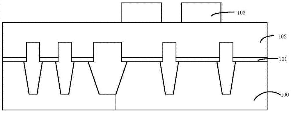
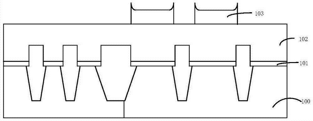
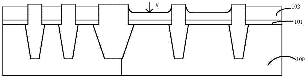
Image

Examples
Embodiment Construction
[0022] In the following description, numerous specific details are given in order to provide a more thorough understanding of the present invention. It will be apparent, however, to one skilled in the art that the present invention may be practiced without one or more of these details. In other examples, some technical features known in the art are not described in order to avoid confusion with the present invention.
[0023] In order to thoroughly understand the present invention, detailed steps will be presented in the following description to illustrate how the present invention solves the problems in the prior art. Apparently, the preferred embodiments of the present invention are described in detail as follows, however, the present invention may also have other implementations apart from these detailed descriptions.
[0024] It should be noted that the terms used herein are for the purpose of describing specific embodiments only, and are not intended to limit exemplary e...
PUM
 Abstract
Description
Claims
Application Information
 - R&D
- Intellectual Property
- Life Sciences
- Materials
- Tech Scout
- Unparalleled Data Quality
- Higher Quality Content
- 60% Fewer Hallucinations
Browse by: Latest US Patents, China's latest patents, Technical Efficacy Thesaurus, Application Domain, Technology Topic, Popular Technical Reports.
© 2025 PatSnap. All rights reserved.Legal|Privacy policy|Modern Slavery Act Transparency Statement|Sitemap|About US| Contact US: help@patsnap.com