Method for etching surface insulation layer of PAD at bottom of TSV hole of CIS product

A technology for insulating layers and products, applied in electrical components, semiconductor/solid-state device manufacturing, circuits, etc., can solve problems such as difficulty in exposure and development, inconsistent thickness of photoresist, and difficulty in detecting the complete development of the bottom, so as to save yellow light process , The effect of saving process cost

Inactive Publication Date: 2015-05-06
NAT CENT FOR ADVANCED PACKAGING
View PDF4 Cites 6 Cited by
  • Summary
  • Abstract
  • Description
  • Claims
  • Application Information

AI Technical Summary

Problems solved by technology

[0005] 1) The photoresist coating process is generally carried out by spraying glue. This method will cause the thickness of the photoresist at the bottom of the TSV hole, the side wall and the edge of the upper opening to be inconsistent, so that it should not be etched in the subsequent etching process. The eclipsed area, especially the edge of the upper opening of the TSV hole, is damaged because the light cannot be blocked;
[0006] 2) As the depth of the TSV hole becomes deeper and the aperture becomes smaller, the exposure and development on the PAD at the bottom of the TSV hole will become more and more difficult, and it will be difficult to detect whether the bottom is completely developed after development. Once there is photoresist remaining on the insulating layer on the surface of the PAD, the removal of the insulating layer will fail this time, eventually leading to the failure of the interconnection
[0008] Dry etching also has a load effect, that is, the etching rate on the back surface of the wafer is fast, and the etching rate at the bottom of the TSV hole is slow. In order to ensure that the insulating layer at the bottom of the TSV hole is completely removed, it is necessary to over-etch the bottom of the TSV hole , and over-etching will also speed up the removal rate of the insulating layer on the back surface of the wafer, which may eventually cause some areas on the back surface of the wafer, especially the insulating layer on the upper opening edge of the TSV hole, to be etched away, causing insulation failure and increasing If the upper surface is covered with the thickness of the insulating layer, the thickness of the insulating layer at the bottom of the TSV hole will also increase, which increases the difficulty of the etching process

Method used


Image

  • Method for etching surface insulation layer of PAD at bottom of TSV hole of CIS product
  • Method for etching surface insulation layer of PAD at bottom of TSV hole of CIS product
  • Method for etching surface insulation layer of PAD at bottom of TSV hole of CIS product

Examples


Embodiment Construction

[0031] The present invention will be described in detail below in conjunction with specific embodiments shown in the accompanying drawings. However, these embodiments do not limit the present invention, and any structural, method, or functional changes made by those skilled in the art according to these embodiments are included in the protection scope of the present invention.

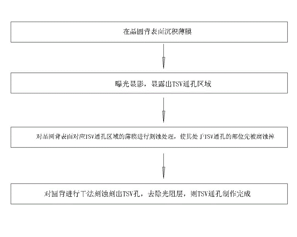
[0032] figure 1 Shown is the flow chart of the etching method of the PAD surface insulating layer at the bottom of the TSV hole of the CIS product involved in the present invention.

[0033] A kind of etching method of PAD surface insulation layer at bottom of CIS product TSV hole of the present invention, it comprises following specific steps:

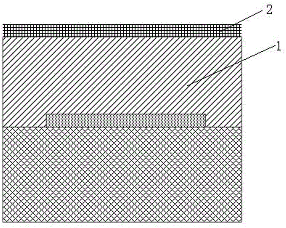
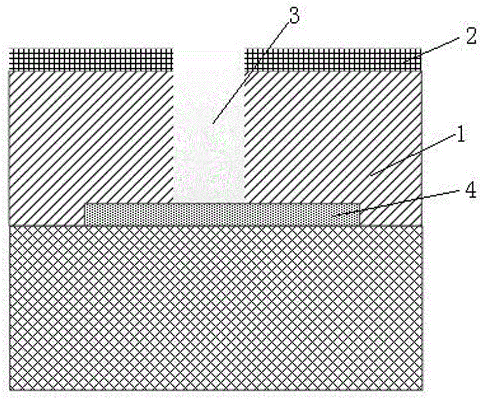
[0034] (1), see figure 2 , first deposit a layer of first insulating layer 2 on the wafer 1 surface where the TSV holes are to be etched;

[0035] Deposit a layer of first insulating layer on the surface of the TSV wafer to be opened. The insulating layer ...


PUM


Abstract

The invention discloses a method for etching a surface insulation layer of a PAD at a bottom of a TSV (Temperature Safety Valve) hole of a CIS (Cartographic Information System) product. The method comprises the following steps: (1) before the TSV hole is etched on the back of the wafer, and a first insulation layer is firstly deposited; (2) photo-etching and dry etching processes are continuously performed to the TSV hole to etch the TSV hole; (3) after the TSV hole is deposited, a second insulation layer is continuously etched; (4) the dry etching process is performed to the whole back surface of the wafer until the insulation layer on the PAD at the bottom of the TSV hole is totally etched. The advantage of the method lies in that the first insulation layer firstly deposited may be regarded as the second insulation layer on the subsequent PAD, removed and used as a barrier layer, when the second insulation layer on the subsequent PAD is etched, the first insulation layer on the back surface of the wafer isn't worried about being destroyed, the photo-etching process with relatively high process difficulty is omitted and the process cost is saved.

Description

technical field [0001] The invention relates to the technical field of semiconductors, in particular to an etching method for an insulating layer on a PAD surface at the bottom of a TSV hole of a CIS product. Background technique [0002] With the development of semiconductor technology, the feature size of integrated circuits continues to shrink, and the interconnection density of devices continues to increase. Especially for CIS products, the pixels are getting bigger and bigger, from the initial million level to the current tens of millions level, so the traditional two-dimensional packaging can no longer meet the needs of the industry. Therefore, the stacked packaging method based on TSV vertical interconnection has its advantages The key technical advantages of short-distance interconnection and high-density integration have gradually led the development trend of packaging technology. [0003] TSV technology includes the following key processes: through-hole etching, i...

Claims


Application Information

Patent Timeline
Patent Type & Authority Applications(China)
IPC IPC(8): H01L21/768
CPCH01L21/768H01L21/311H01L21/31116H01L21/31138
Inventor 冯光建张文奇
Owner NAT CENT FOR ADVANCED PACKAGING
Why Eureka
Try Eureka