LED chip structure and preparation method thereof

A light-emitting diode and chip structure technology, which is applied in the direction of electrical components, circuits, semiconductor devices, etc., can solve the problems of the decrease of the effective area of ​​light output, the reduction of the brightness and luminous efficiency of light-emitting diodes, and achieve the improvement of brightness and luminous efficiency, and the increase of effective luminous area. The effect of large and small area

Inactive Publication Date: 2015-05-06
WUXI CHINA RESOURCES HUAJING MICROELECTRONICS
View PDF12 Cites 8 Cited by
  • Summary
  • Abstract
  • Description
  • Claims
  • Application Information

AI Technical Summary

Problems solved by technology

[0004] figure 2 shows the lateral structure of light emitting diodes in the prior art along figure 1 Medium AA 1 Sectional view of direction, from figure 2 It can be found that when making the N electrode 15, the quantum well active layer 13 and the p-type gallium nitrid

Method used


Image

  • LED chip structure and preparation method thereof
  • LED chip structure and preparation method thereof
  • LED chip structure and preparation method thereof

Examples


Embodiment Construction

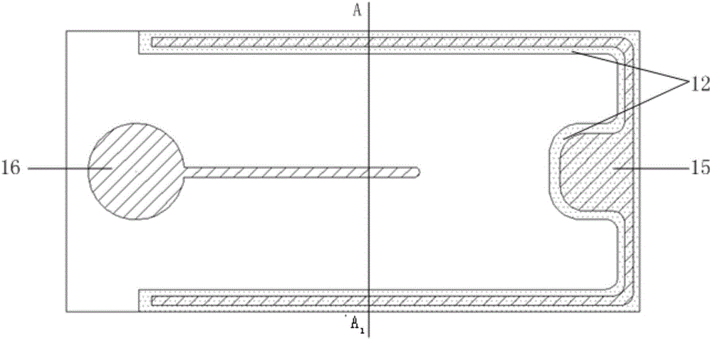
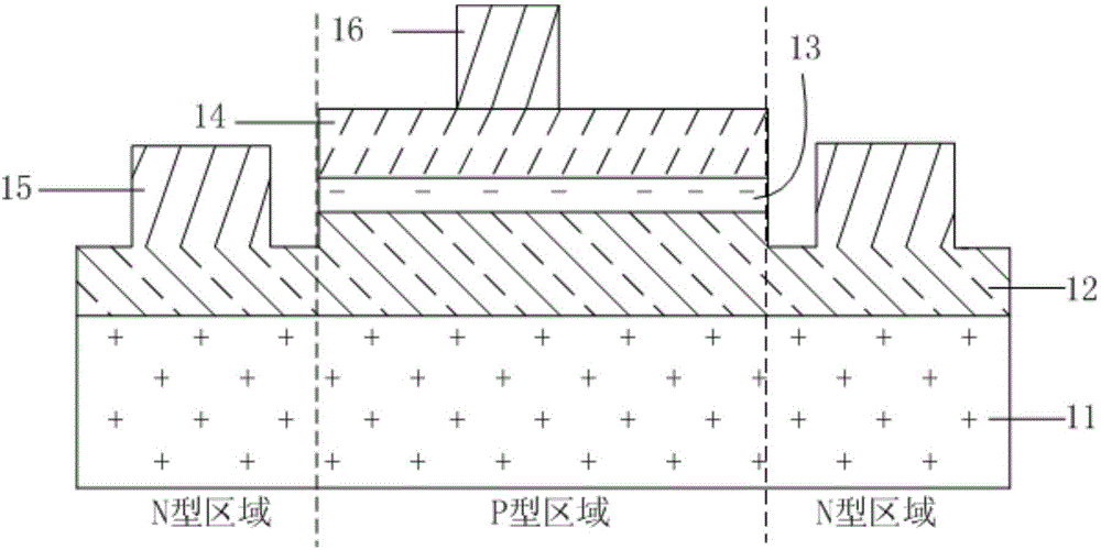
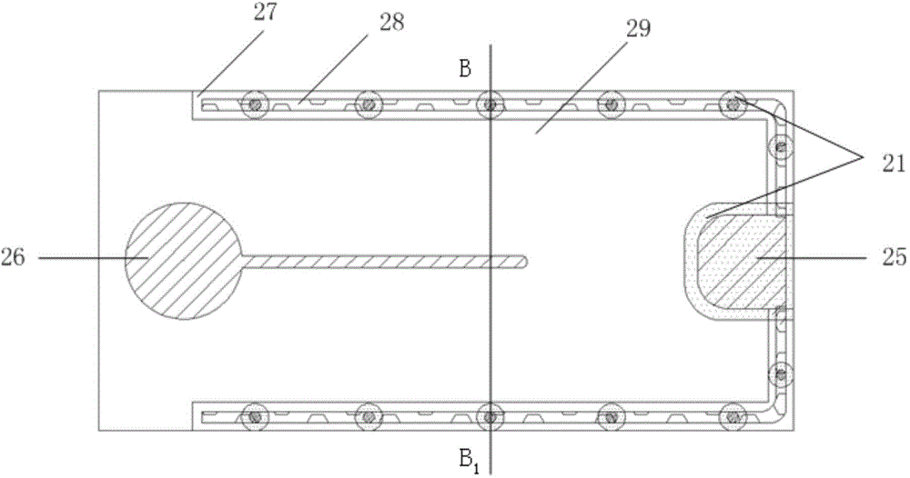
[0043] The present invention will be further described in detail below in conjunction with the accompanying drawings and embodiments. It should be understood that the specific embodiments described here are only used to explain the present invention, but not to limit the present invention. In addition, it should be noted that, for the convenience of description, only parts related to the present invention are shown in the drawings but not all content.

[0044] Embodiments of the present invention provide a light-emitting diode chip structure and a preparation method thereof. Since the structure of the light-emitting diode chip is improved, the light-emitting area is increased, and the luminous efficiency is improved. The light-emitting diode chip can be used in light-emitting diodes with lighting and display functions , the light-emitting diodes include but are not limited to, for example: can be LED energy-saving lamps, LED flashlights, LED decorative lights, LED outdoor larg...


PUM


Abstract

The invention discloses an LED chip structure and a preparation method thereof. The LED chip structure comprises a substrate, and an epitaxial layer positioned on the substrate; the epitaxial layer comprises a first area layer, a quantum well active layer and a second area layer. The LED chip structure further comprises a slot which extends from the second area layer to the second area layer or extending into the first area layer, a first electrode which is formed in the slot and in contact with the first area layer, and a second electrode which is formed on the second area layer. According to the LED chip structure, the area of an etching are of an LED chip can be reduced, the effective lighting area of the LED chip can be increased, and as a result, the lighting efficiency is increased.

Description

technical field [0001] The invention relates to the technical field of semiconductors, in particular to the technical field of power semiconductor devices, in particular to a light emitting diode chip structure and a preparation method thereof. Background technique [0002] Light Emitting Diodes (LED for short) is a semiconductor electronic component that can emit light. With the advantages of no pollution sources of mercury and other toxic substances, with the promotion of light-emitting diodes, its structure has become more and more, and its brightness has become brighter and brighter. [0003] figure 1 A front top view of a lateral structure of a light emitting diode chip in the prior art is shown. The two electrodes of the light-emitting diode chip with a lateral structure are on the same side of the light-emitting diode chip, the P electrode 16 is in the P-type gallium nitride region of the light-emitting diode epitaxial layer, and the N electrode 15 is distributed in...

Claims


Application Information

Patent Timeline
IPC IPC(8): H01L33/20H01L33/38H01L33/00
CPCH01L33/20H01L33/007H01L33/382
Inventor 王磊王强巩春梅朱琳
Owner WUXI CHINA RESOURCES HUAJING MICROELECTRONICS
Why Eureka
Try Eureka