Flip LED (light-emitting diode) substrate structure

A technology for LED substrates and LED chips, applied in electrical components, circuits, semiconductor devices, etc., can solve problems such as a large amount of solder and high consumption of precious metals

Inactive Publication Date: 2015-05-06
SHANGHAI UNIV
View PDF3 Cites 8 Cited by
  • Summary
  • Abstract
  • Description
  • Claims
  • Application Information

AI Technical Summary

Problems solved by technology

For example, a large amount of solder is required for soldering, and a large amount of precious metal is consumed for gold wire soldering, etc.

Method used


Image

  • Flip LED (light-emitting diode) substrate structure
  • Flip LED (light-emitting diode) substrate structure
  • Flip LED (light-emitting diode) substrate structure

Examples


Embodiment Construction

[0022] The structure of the flip-chip LED substrate will be further described in detail below with reference to the implementation manner and the accompanying drawings.

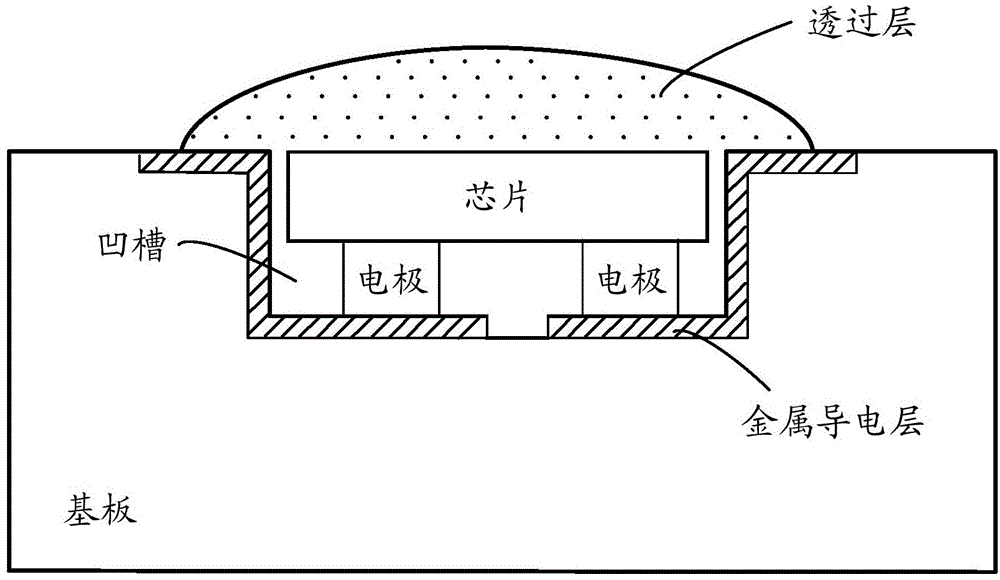
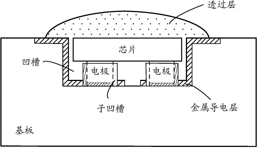
[0023] combined with figure 1 , In the flip-chip LED substrate structure according to one embodiment, grooves are provided on the substrate, and the grooves can accommodate LED chips. The conductive metal layer is arranged in the groove and extends to the surface of the substrate. In addition, the conductive metal layer is divided into two parts, which are respectively connected to two electrodes of the LED chip. A light-transmitting layer is covered on the top of the LED chip, and the light-transmitting layer can be made of highly transparent materials such as epoxy resin, polycarbonate, polymethyl methacrylate, glass, and organic silicon materials. The flip-chip LED substrate structure of this scheme cleverly uses the light-transmitting layer to cover and press down on the LED chip, and makes the LED chip ...


PUM


Abstract

The invention discloses a flip LED (light-emitting diode) substrate structure. The flip LED substrate includes a groove which is arranged on a substrate and used for holding LED chips; conductive metal layers which are arranged on the groove and extended to the surface of the substrate, wherein there are two conductive metal layers which are respectively connected with two electrodes of the LED chips; a transparent layer which covers the LED chips. According to the flip LED substrate structure, the transparent layer is ingeniously utilized to cover and press on the LED chips, the LED chips are electrically connected with the metal layers, soldering flux is coated without a silk-screen printing process, and the LED chips are directly placed in the groove; moreover, the procedure of gold line bonding is reduced, and the LED packaging efficiency is improved; meanwhile, a lot of money is saved and cost is reduced.

Description

technical field [0001] The invention relates to the technical field of LED packaging, in particular to a flip-chip LED substrate structure. Background technique [0002] LED (Light Emitting Diode), light-emitting diode, is a solid-state semiconductor device that can convert electrical energy into visible light. In order for LEDs to eventually be used in daily life, LEDs need to be packaged. [0003] The packaging of LED chips, including packaging materials, wires, substrates, etc., also requires a variety of processes to achieve packaging. For example, a large amount of solder is required for soldering, and a large amount of precious metal is consumed for gold wire soldering. Reducing the use of solder and precious metals and reducing costs are important technical problems in this technical field. Contents of the invention [0004] Based on this, there is provided a flip-chip LED substrate structure that reduces the use of solder and precious metals. [0005] A flip-ch...

Claims


Application Information

Patent Timeline
Patent Type & Authority Applications(China)
IPC IPC(8): H01L33/48H01L33/62H01L33/60H01L33/64
CPCH01L33/48H01L33/62
Inventor 张建华殷录桥白杨南婷婷
Owner SHANGHAI UNIV
Why Eureka
Try Eureka