Manufacturing method of backside image sensor

An image sensor, back-illuminated technology, used in semiconductor/solid-state device manufacturing, radiation control devices, electrical components, etc., can solve the problems of poor optoelectronic characteristics and output quality, high manufacturing costs, and complex manufacturing methods.

Inactive Publication Date: 2015-05-13
WUHAN XINXIN SEMICON MFG CO LTD
View PDF6 Cites 13 Cited by
  • Summary
  • Abstract
  • Description
  • Claims
  • Application Information

AI Technical Summary

Problems solved by technology

[0007] In view of the above problems, the present invention provides a method for preparing a back-illuminated image sensor to solve the defects in the prior art that the prep

Method used


Image

  • Manufacturing method of backside image sensor
  • Manufacturing method of backside image sensor
  • Manufacturing method of backside image sensor

Examples


Embodiment Construction
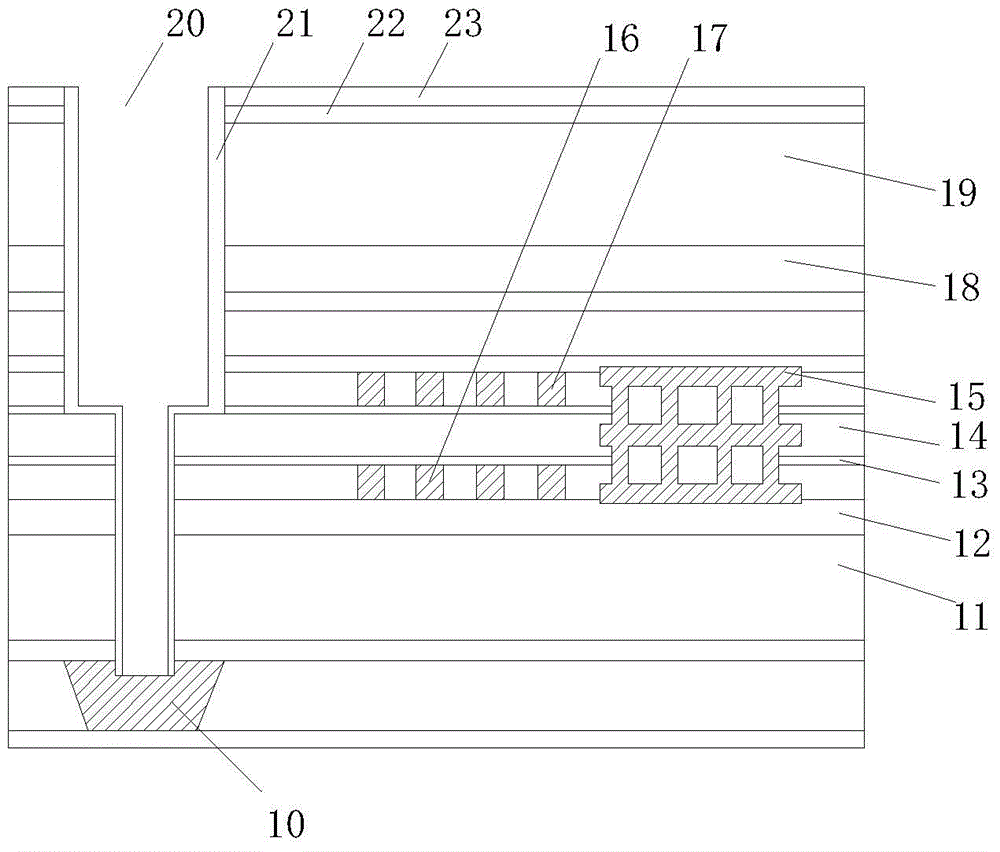
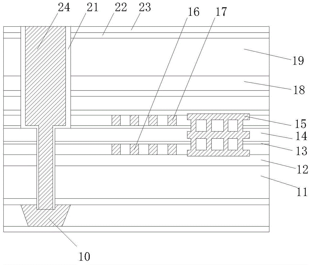
[0040] The core idea of ​​the present invention is to integrate the metal leads of the back-illuminated image sensor with the Pad, and simultaneously prepare the metal isolation barrier to provide the basis for the subsequent color filter buried process, thereby improving the simplification of the image sensor manufacturing process , reduce the preparation cost and improve the output image quality.

[0041] The present invention will be further described below in conjunction with the accompanying drawings and specific embodiments, but not as a limitation of the present invention.

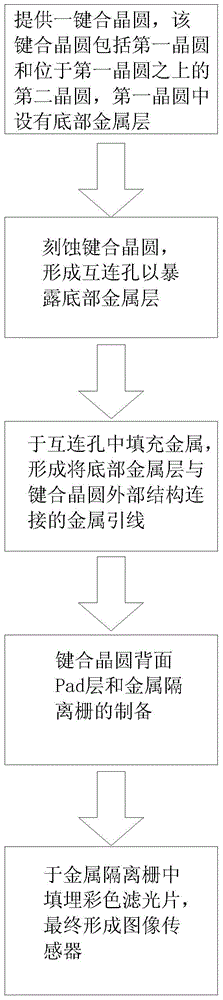
[0042] Such as figure 1 Shown is the flow chart of the preparation method of the back-illuminated image sensor in the embodiment of the present invention. First, provide a bonded wafer with a photosensitive area (that is, a metal isolation barrier and a buried color filter area) and a bottom metal layer; secondly, etch the bonded wafer to form an exposed bottom metal layer. Interconnect holes on t...


PUM


Abstract

The invention refers to the technical field of semiconductor manufacturing, and particularly relates to a manufacturing method of a backside image sensor. The manufacturing method of the backside image sensor comprises the steps: forming an interconnection hole through etching a bonded wafer, and filling a metal to form a metal lead; meanwhile, synchronously preparing a metal isolating grid and a Pad layer contacted with the metal lead at the back side of the bonded wafer, and then embedding a color filter in the metal isolating grid. According to the manufacturing method of the backside image sensor, a metal layer in the bonded wafer can be derived and integrated with the Pad, thus requirements of simple and low-cost manufacturing technique can be realized on a certain extent; meanwhile, the metal isolating grid synchronously prepared with the Pad provides a good embedding environment for the subsequent color filter, a light path is minimized, and the optical-electrical characteristic and the output quality of the backside image sensor are greatly improved.

Description

technical field [0001] The invention relates to the technical field of semiconductor manufacturing, in particular to a method for preparing a back-illuminated image sensor. Background technique [0002] With the continuous maturity and development of semiconductor manufacturing technology, image sensors are increasingly used in digital cameras, PC Cameras, video phones, third-generation mobile phones, video conferencing, intelligent security systems, car reversing sensors, toys and industrial, medical, etc. in other fields. [0003] For example, CMOS image sensors are optoelectronic components and CMOS image sensors are gradually becoming the mainstream of image sensors because their manufacturing methods are compatible with existing integrated circuit manufacturing methods, and their performance has many advantages over the original charge-coupled device (CCD). , which can integrate the driving circuit and the pixel, which simplifies the hardware design and reduces the pow...

Claims


Application Information

Patent Timeline
IPC IPC(8): H01L21/50H01L21/60H01L27/146
Inventor 胡思平胡胜董金文
Owner WUHAN XINXIN SEMICON MFG CO LTD
Why Eureka
Try Eureka