Forming method of semiconductor device

A semiconductor and device technology, applied in the field of semiconductor device formation, can solve the problems of semiconductor device leakage, rough sidewalls of through holes, etc.

Inactive Publication Date: 2015-05-13
SEMICON MFG INT (SHANGHAI) CORP
View PDF6 Cites 7 Cited by
  • Summary
  • Abstract
  • Description
  • Claims
  • Application Information

AI Technical Summary

Problems solved by technology

[0006] However, the sidewalls of via holes formed by the existing TSV technology are rough, which easily leads to leakage problems in semiconductor devices

Method used


Image

  • Forming method of semiconductor device
  • Forming method of semiconductor device
  • Forming method of semiconductor device

Examples


Embodiment Construction

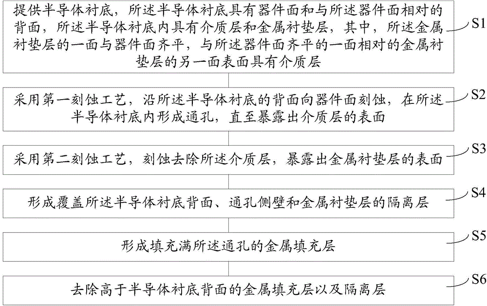
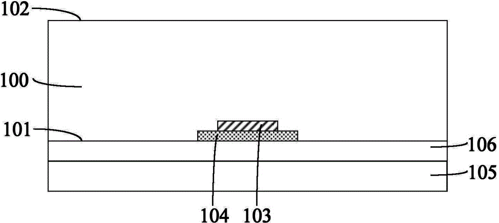
[0033] As mentioned in the background art, the sidewalls of the through holes of the semiconductor device formed in the prior art are rough, which easily leads to the leakage problem of the semiconductor device.

[0034] In order to solve the above problems, the formation method of the semiconductor device is studied. The formation method of the semiconductor device includes the following steps, please refer to figure 1: Step S1, providing a semiconductor substrate, the semiconductor substrate has a device face and a back surface opposite to the device face, a dielectric layer and a metal backing layer are provided in the semiconductor substrate, wherein the metal backing layer One side is flush with the device surface, and the other surface of the metal backing layer opposite to the side flush with the device surface has a dielectric layer; Step S2, using the first etching process, along the back side of the semiconductor substrate Etching the device surface, forming a throug...


PUM


Abstract

The invention provides a forming method of a semiconductor device. The forming method comprises the steps of providing a semiconductor substrate which is provided with a device surface and a back opposite to the device surface, etching the semiconductor substrate in a direction from the back of the semiconductor substrate to the device surface of the semiconductor substrate, forming a through hole in the semiconductor substrate to expose the surface of a dielectric layer, forming an insulating layer for covering the back of the semiconductor substrate, the sidewall of the through hole and the insulating layer of the dielectric layer, and etching off the insulating layer and the dielectric layer located at the bottom of the through hole by use of an anisotropic etching process to expose the surface of a metal liner layer, wherein the dielectric layer and the metal liner layer are formed in the semiconductor substrate; the insulating layer thinnest on the surface of the dielectric layer. The forming method has the advantages that the process of etching off the dielectric layer is prevented from damaging the sidewall of the through hole, the roughness of the sidewall of the through hole is improved, and therefore, the reliability of the semiconductor device can be improved, and the electric leakage problem can be avoided.

Description

technical field [0001] The invention relates to the field of semiconductor manufacturing, in particular to a method for forming a semiconductor device. Background technique [0002] With the rapid development of semiconductor manufacturing technology, in order to achieve faster computing speed, larger data storage capacity and more functions of semiconductor devices, semiconductor chips are developing towards higher integration. The higher the integration level of the semiconductor chip, the smaller the feature size (CD: Critical Dimension) of the semiconductor device. [0003] A three-dimensional integrated circuit (IC: Integrated Circuit) is manufactured by using advanced chip stacking technology, which is to stack chips with different functions into an integrated circuit with a three-dimensional structure. Compared with two-dimensional integrated circuits, the stacking technology of three-dimensional integrated circuits can not only shorten the signal transmission path o...

Claims


Application Information

Patent Timeline
Patent Type & Authority Applications(China)
IPC IPC(8): H01L21/768
CPCH01L21/76801
Inventor 冯霞张海芳刘煊杰吴秉寰
Owner SEMICON MFG INT (SHANGHAI) CORP
Why Eureka
Try Eureka