Power transistor array structure with electrostatic protection circuit integrated

A technology for power transistors and electrostatic protection, applied in circuits, thyristors, electro-solid devices, etc., can solve problems such as easy triggering and reduction of the safe working range of power transistor arrays, reduce false triggering, improve electrostatic protection capabilities, expand The effect of safe working area

Active Publication Date: 2015-05-20
SHANGHAI HUAHONG GRACE SEMICON MFG CORP
View PDF4 Cites 2 Cited by
  • Summary
  • Abstract
  • Description
  • Claims
  • Application Information

AI Technical Summary

Problems solved by technology

Although embedding SCR can effectively improve the electrostatic protection capability of the output power transistor array, it will be a technical difficulty in this design to avoid false triggering of the SCR when the power transistor array is working normally. The higher the voltage and the higher the current, the easier it is for the SCR to trigger , so the embedded SCR will reduce the safe operating range (SOA) of the power transistor array

Method used


Image

  • Power transistor array structure with electrostatic protection circuit integrated
  • Power transistor array structure with electrostatic protection circuit integrated
  • Power transistor array structure with electrostatic protection circuit integrated

Examples


Embodiment Construction

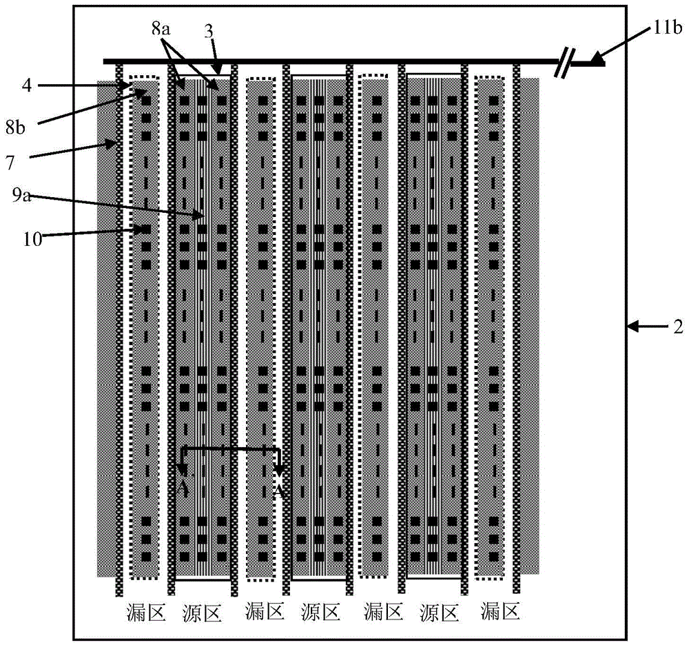
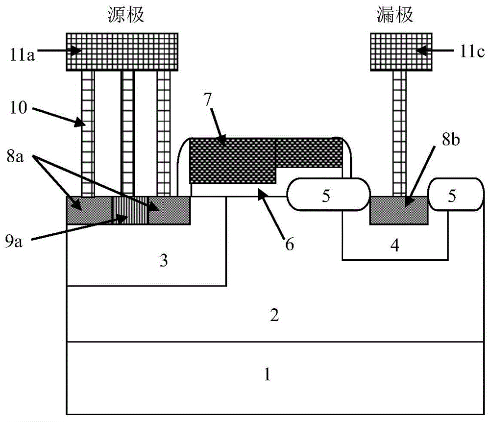
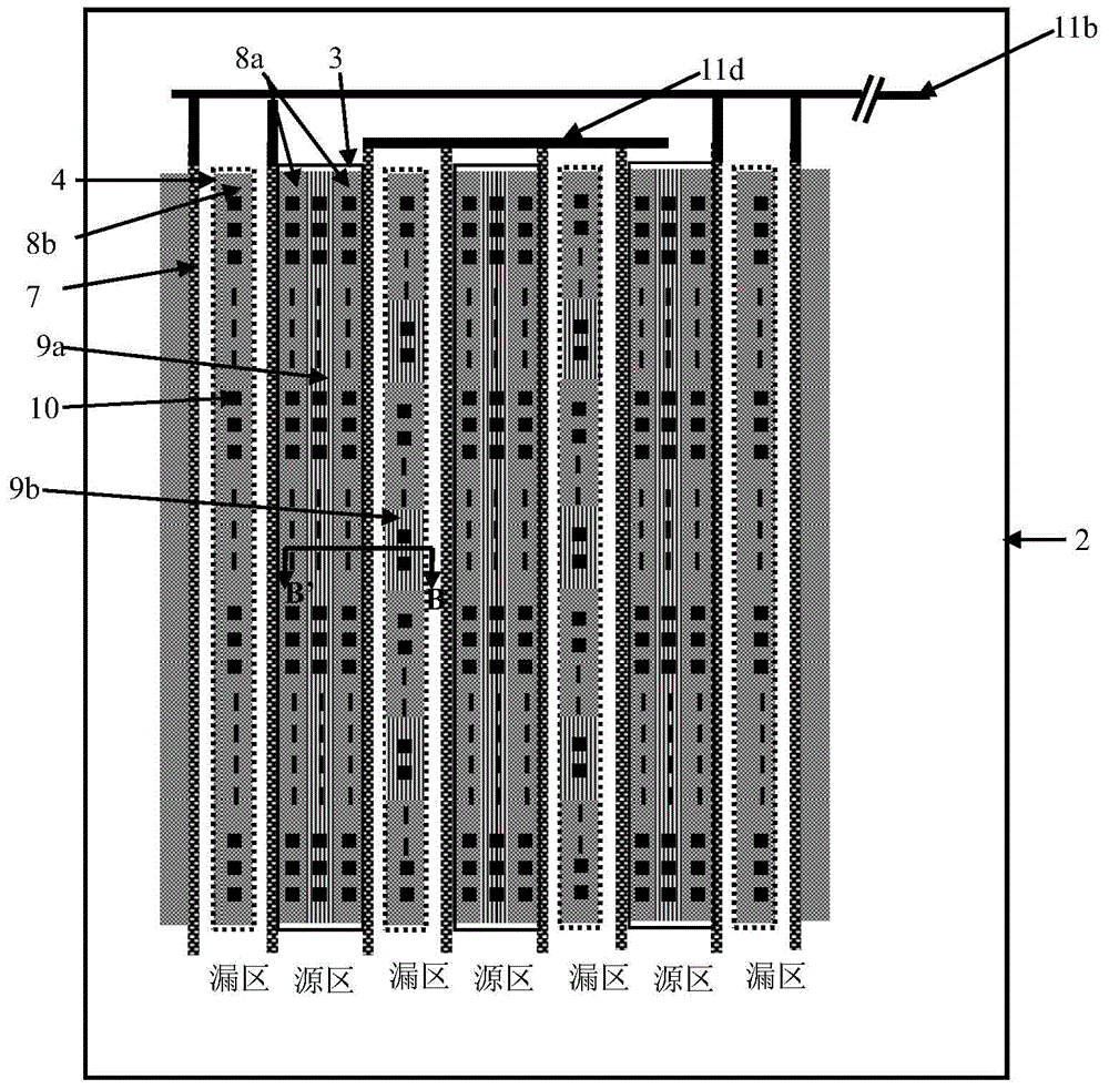
[0038] Such as Figure 2A As shown, it is a schematic diagram of a layout structure of a power transistor array according to an embodiment of the present invention; Figure 2B shown, is along the Figure 2A Schematic diagram of the cross-sectional structure of the unit structure at the B'B position of ; a deep N well (DNW) 2 is formed on the silicon substrate 1, and the entire power transistor array is formed in the deep N well 2, and the unit of the power transistor Structure one is the NLDMOS device structure, including:

[0039] A P-type body region 3 formed in the deep N well 2 .

[0040] An N well 4 is formed in the deep N well 2 and is separated from the P-type body region 3 by a certain distance.

[0041] The drain region 8b is composed of the N+ region formed in the N well 4; a field oxygen layer 5 is formed between the drain region 8b and the P-type body region 3, and the drain region 8b and the field The oxygen layer 5 is self-aligned.

[0042]The source region ...


PUM


Abstract

The invention discloses a power transistor array structure with an electrostatic protection circuit integrated. Embedding of an electrostatic protection circuit formed by an SCR (silicon controlled rectifier) can be realized by partially replacing region sections of a drain region of a first unit structure of a power transistor with a region P+, and a grid electrode of the SCR is not connected with a grid electrode of the first unit structure but connected with a source electrode of the first unit structure. On the premise that performances of a power transistor array are unaffected and the process is unchanged, electrostatic protection capability of the power transistor array can be improved, false triggering accidents of the silicon controlled rectifier can be effectively reduced, and accordingly safety operation range of the power transistor array can be expanded. In addition, a grid gate structure of the SCR is designed to be recessed towards a drain side, and the region P+ is injected to a body region of a source side, so that the false triggering accidents of the silicon controlled rectifier can be further reduced, and the safety operation range of the power transistor array can be further expanded.

Description

technical field [0001] The invention relates to a semiconductor integrated circuit, in particular to a power transistor array structure integrated with an electrostatic protection circuit. Background technique [0002] Power transistors are often used in high-voltage integrated circuits as output drive tubes that drive relatively large currents. Existing power drive tubes generally appear in the form of arrays. Such as Figure 1A Shown is a schematic diagram of the existing power transistor array layout structure; Figure 1B is along Figure 1A Schematic diagram of the cross-sectional structure of the unit structure at position A'A of ; a deep N well (DNW) 2 is formed on the silicon substrate 1, and the entire power transistor array is formed in the deep N well 2, and the unit of the power transistor Structure one is the NLDMOS device structure, including: [0003] A P-type body region 3 formed in the deep N well 2 . [0004] An N well 4 is formed in the deep N well 2 and...

Claims


Application Information

Patent Timeline
Patent Type & Authority Applications(China)
IPC IPC(8): H01L27/02H01L29/74H01L29/423
Inventor 武洁
Owner SHANGHAI HUAHONG GRACE SEMICON MFG CORP
Why Eureka
Try Eureka