Eureka AIR delivers breakthrough ideas for toughest innovation challenges, trusted by R&D personnel around the world.

Structure of a superjunction mosfet device

A super junction and device technology, used in semiconductor devices, electrical components, circuits, etc., can solve the problems of poor device stability, relatively large breakdown voltage fluctuations, and difficulty in controlling the stability of doping concentration of super junction MOSFETs. Very poor, improved uniformity effect

Active Publication Date: 2018-04-17
SHANGHAI HUAHONG GRACE SEMICON MFG CORP
View PDF6 Cites 0 Cited by
  • Summary
  • Abstract
  • Description
  • Claims
  • Application Information

AI Technical Summary

Problems solved by technology

[0004] However, it is difficult to control the stability of the doping concentration of the super junction MOSFET
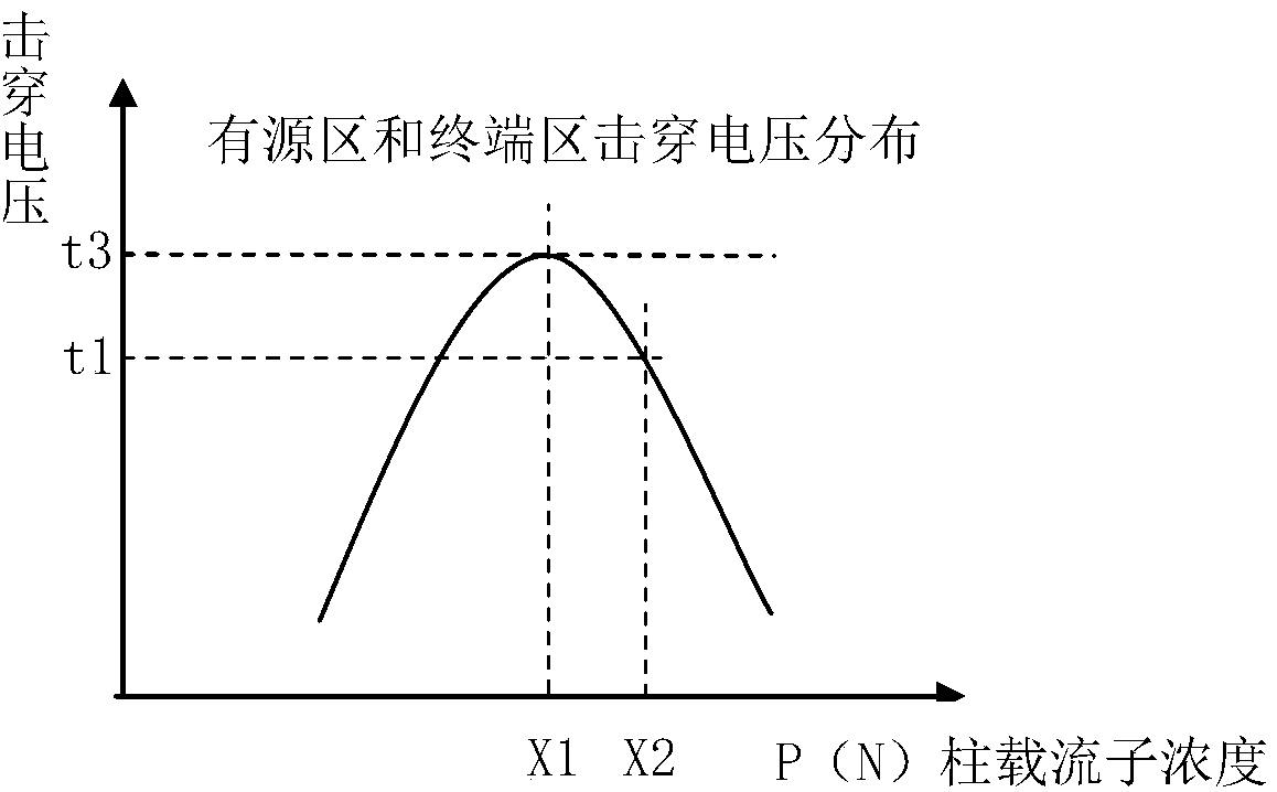
Usually, the P / N width ratio of the active region and the terminal region of the device are consistent, and the breakdown voltage distributions of the active region and the terminal region are also consistent (see figure 1 ), the breakdown voltage of the device depends on the breakdown voltage of one of them, which is t3 to t1, which leads to a relatively large fluctuation of the breakdown voltage and poor stability of the device

Method used


Image

  • Structure of a superjunction mosfet device
  • Structure of a superjunction mosfet device
  • Structure of a superjunction mosfet device

Examples


Embodiment Construction

[0022] In order to have a more specific understanding of the technical content, characteristics and effects of the present invention, now in conjunction with the illustrated embodiment, the details are as follows:

[0023] See Figure 2-5 Shown, the superjunction MOSFET device of the present invention, its specific manufacturing process steps are:

[0024] Step 1, growing a first semiconductor layer with a thickness of 10-100 microns on the semiconductor substrate, such as figure 2 As shown, and grow a layer of dielectric film on the first semiconductor layer (not shown in the figure).

[0025] The first semiconductor layer and the semiconductor substrate have a first doping type. A typical first semiconductor layer is an N-type silicon epitaxial layer, and a typical semiconductor substrate is an N-type silicon substrate. The doping concentration of the first semiconductor layer is set to m. The carrier concentration of the semiconductor base is higher than that of the fi...


PUM


Abstract

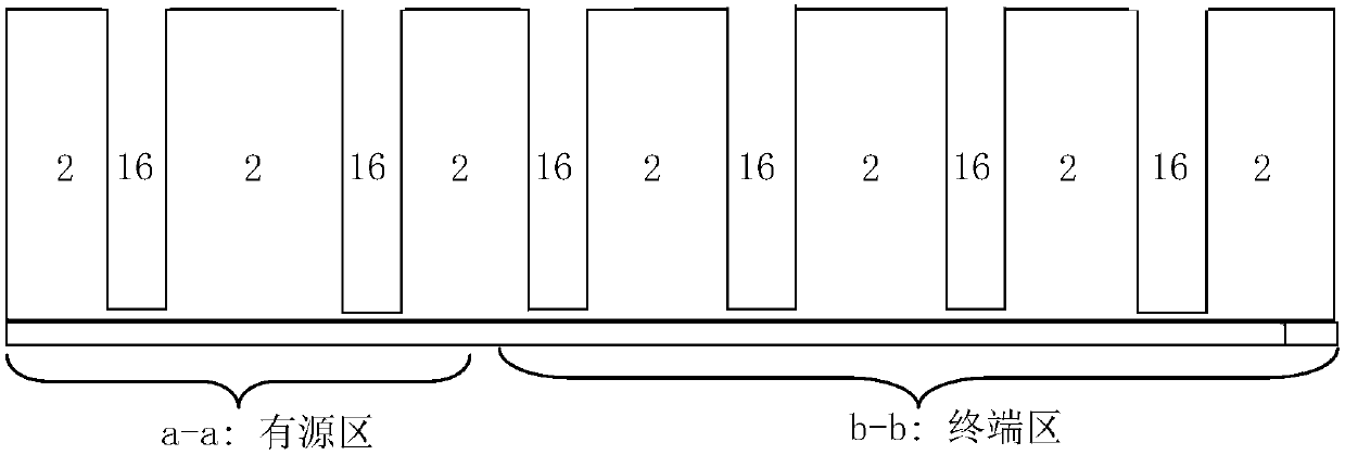
The invention discloses a structure of a super junction MOSFET device, wherein the width ratio S1 of the first semiconductor layer and the second semiconductor layer in the active region, the width ratio S2 of the first semiconductor layer and the second semiconductor layer in the terminal region, and the active region and the doping concentration m of the first semiconductor layer in the terminal area, and the doping concentration n of the second semiconductor layer in the active area and the terminal area, satisfying the conditions: 0<1‑S1m / n≤0.1 and‑0.1≤1‑S2m / n <0; or -0.1≤1‑S1m / n<0 and 0<1‑S2m / n≤0.1. In the present invention, the width ratio and doping concentration ratio of the first semiconductor layer and the second semiconductor layer in the active region and the terminal region are reasonably designed, so that the breakdown voltage of the active region and the terminal region is distributed in a certain difference range In this way, the breakdown voltage range is reduced, and the uniformity of breakdown voltage and the uniformity of super junction MOSFET devices are improved.

Description

technical field [0001] The invention relates to the field of integrated circuit manufacturing, in particular to the structure of a super junction MOSFET device. Background technique [0002] VDMOSFET (vertical double-diffused MOS transistor) can reduce the on-resistance by reducing the thickness of the drain drift region. However, reducing the thickness of the drain drift region will reduce the breakdown voltage of the device. Therefore, in VDMOS, increase The breakdown voltage of the device and the reduction of the on-resistance of the device are a pair of contradictions. [0003] The super junction MOSFET adopts a new voltage-resistant layer structure, which uses a series of alternately arranged P-type and N-type semiconductor thin layers to deplete the P-type and N-type regions at a lower reverse voltage to achieve mutual charge compensation. As a result, the P-type and N-type regions can achieve high breakdown voltage under high doping concentration, so that low on-resi...

Claims


Application Information

Patent Timeline
Patent Type & Authority Patents(China)
IPC IPC(8): H01L29/78H01L29/06
Inventor 刘继全
Owner SHANGHAI HUAHONG GRACE SEMICON MFG CORP
Why Eureka
Eureka Blog
Learn More