

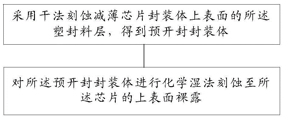
Opening method of chip packages
A chip packaging and packaging technology, applied in semiconductor/solid-state device manufacturing, electrical components, circuits, etc., can solve problems such as chip and lead damage, and achieve the effect of improving and avoiding damage.
- Summary
- Abstract
- Description
- Claims
- Application Information
AI Technical Summary
Problems solved by technology
Method used
Image

Examples
Embodiment 1
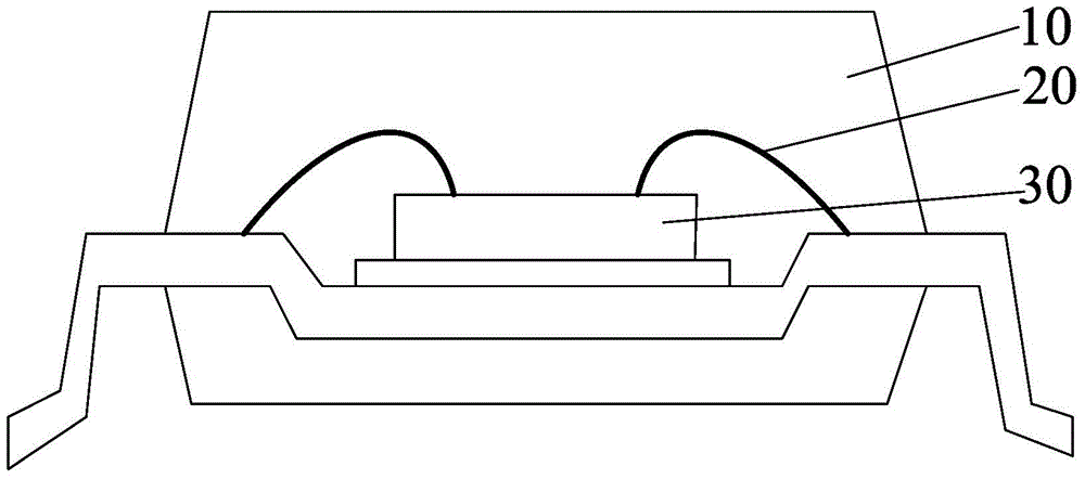
[0044] A plasma etching machine model of Plasma lab80plus was used as the dry etching device, the excitation power of the plasma etching machine was set to 1000W, the bias voltage was 500V, and the etching gas was Ar and o 2 , the pressure of the etching gas is 100mT, the flow rate is 1000sccm, the etching time is 20min, and the etching rate is about 25μm / min. The thickness of the etched plastic compound layer is calculated by the etching rate and etching time. The distance from the top surface of the etched plastic compound layer to the highest point of the lead is 20 μm.
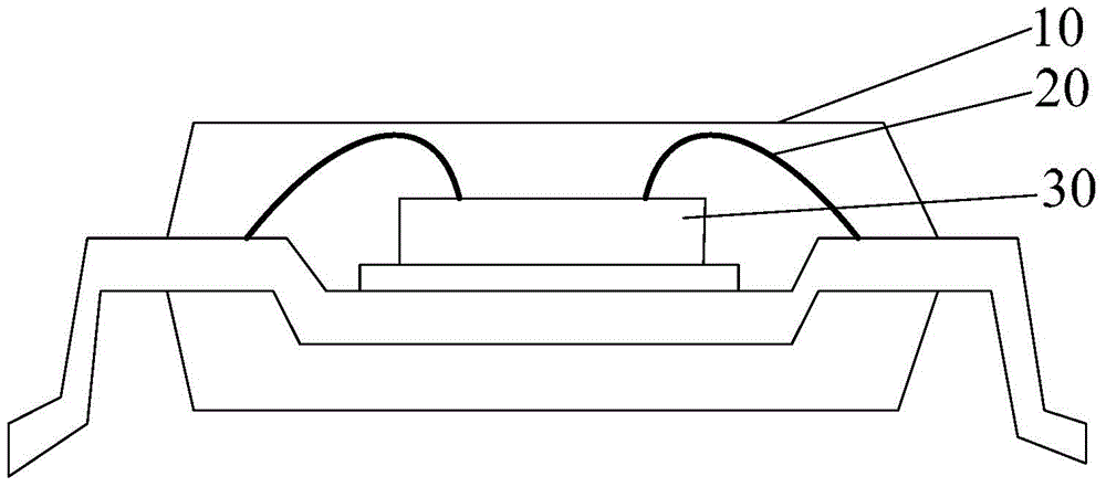
[0045] The unsealing device disclosed in the patent application with application number 200910056017.8 is used for chemical wet etching, wherein the etching solution is a mixed acid solution composed of fuming nitric acid and 98% sulfuric acid with a volume ratio of 1:1, and the etching temperature is After 35° C. for 500 s, the upper surface of the chip was exposed and cleaned with deionized water to obt...
Embodiment 2
[0047] A plasma etching machine model of Plasma lab80plus was used as the dry etching device, the excitation power of the plasma etching machine was set to 1500W, the bias voltage was 100V, and the etching gas was Ar and Ar with a volume ratio of 6:3. O2, the pressure of the etching gas is 200mT, the flow rate is 800sccm, the etching time is 25min, and the etching rate is about 22μm / min. Calculate the thickness of the etched plastic compound layer according to the etching rate and etching time. The distance from the top surface of the etched plastic encapsulant layer to the highest point of the lead is 12 μm.
[0048] The unsealing device disclosed in the patent application with application number 200910056017.8 is used for chemical wet etching, wherein the etching solution is a mixed acid solution composed of fuming nitric acid and 98% sulfuric acid with a volume ratio of 1:3, and the etching temperature is After 40° C. for 500 s, the upper surface of the chip was exposed and...
Embodiment 3
[0050] A plasma etching machine model Plasma lab80plus was used as the dry etching device, the excitation power of the plasma etching machine was set to 600W, the bias voltage was 800V, and the etching gas was Ar and Ar with a volume ratio of 4:1. O2, the pressure of the etching gas is 50mT, the flow rate is 1500sccm, the etching time is 15min, and the etching rate is about 30μm / min. Calculate the thickness of the etched plastic compound layer by the etching rate and etching time. The top surface of the etched plastic encapsulant layer is 30 μm away from the highest point of the lead.
[0051] The unsealing device disclosed in the patent application with application number 200910056017.8 is used for chemical wet etching, wherein the etching solution is a mixed acid solution composed of fuming nitric acid and 98% sulfuric acid with a volume ratio of 1:2, and the etching temperature is After 30° C. for 600 s, the upper surface of the chip is exposed and cleaned with deionized wa...
PUM
 Abstract
Description
Claims
Application Information