Etching method and semiconductor device

A semiconductor and etching technology, applied in the direction of semiconductor devices, semiconductor/solid-state device manufacturing, electrical components, etc., can solve problems affecting the performance of semiconductor devices, production decline, etc., to avoid production decline, avoid residual problems, and reduce the effect of probability of occurrence

Active Publication Date: 2015-05-27
SEMICON MFG INT (SHANGHAI) CORP
View PDF6 Cites 1 Cited by
  • Summary
  • Abstract
  • Description
  • Claims
  • Application Information

AI Technical Summary

Problems solved by technology

[0009] However, in the actual process, after the etching step, there are residues in the trench 10 (such as figure 2 shown in Residue 15), which

Method used


Image

  • Etching method and semiconductor device
  • Etching method and semiconductor device
  • Etching method and semiconductor device

Examples


Embodiment Construction

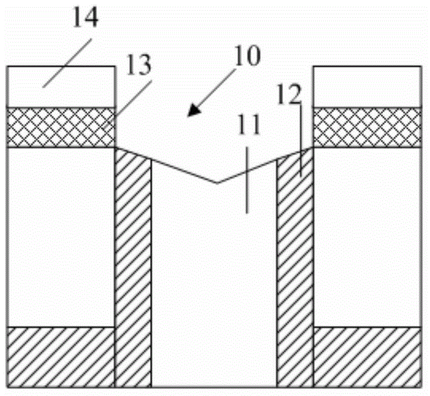
[0030] In the prior art, when the semiconductor layer stack structure is etched, residues are easily generated, and the residues may affect the performance of the semiconductor device, and even lead to a decrease in the yield of the semiconductor device.

[0031] In order to reduce the residues, the materials and causes of the residues are analyzed. Combine below figure 2 , combined with the figure 2 Analysis of semiconductor devices.

[0032] During the process of etching to form the trench 10 , the etching rates of the first semiconductor layer and the second semiconductor layer are different, and an etching gas is used in the etching to form a polymer on the sidewall of the semiconductor layer with a slower etching rate.

[0033] The polymer is equivalent to a small mask. During the etching process, the polymer is used as a mask for etching. The semiconductor layer located under the polymer is not easily removed and remains at the bottom of the trench 10 to form a resid...


PUM


Abstract

The invention provides an etching method and a semiconductor device. The etching method comprises the following steps: providing a substrate; forming a semiconductor layer stacking structure on the substrate, wherein the semiconductor layer stacking structure comprises at least two semiconductor layers arranged in parallel on the substrate and contacting each other; performing first etching on the semiconductor layer stacking structure to realize patterning; and performing second etching on the semiconductor layer stacking structure to remove a polymer formed at the interface of the semiconductor layers through the first etching. The invention further provides the semiconductor device which is formed by the etching method. The performance and output of the semiconductor device can be improved.

Description

technical field [0001] The present invention relates to the technical field of semiconductors, and in particular, to an etching method and a semiconductor device. Background technique [0002] Etching is one of the most commonly used processes in the field of semiconductor technology. Typically used in conjunction with an exposure process to pattern layers. Common etchings include: wet etching and dry etching. [0003] refer to figure 1 , which is a schematic diagram of the structure of a semiconductor device formed by dry etching. The semiconductor device includes: [0004] base (not shown); [0005] The first semiconductor layer 11 and the second semiconductor layer 12 are located on the substrate; the first semiconductor layer 11 and the second semiconductor layer 12 are arranged in parallel on the substrate and are in contact to form a side-by-side stack structure of semiconductor layers, specifically, The first semiconductor layer 11 is a silicon germanium layer, ...

Claims


Application Information

Patent Timeline
IPC IPC(8): H01L21/28H01L29/06
CPCH01L21/30604H01L29/0684
Inventor 马军德郭亮良汪新学阮炯明
Owner SEMICON MFG INT (SHANGHAI) CORP
Why Eureka
Try Eureka