Method for manufacturing color filter substrate

A technology of color filter and manufacturing method, which is applied in the direction of optical filter, photographic plate-making process of pattern surface, optics, etc., can solve problems such as unevenness of the surface of the flat layer, affecting the display quality of the liquid crystal display panel, etc., to avoid the surface Unevenness, the effect of improving display quality

Inactive Publication Date: 2015-06-03
TCL CHINA STAR OPTOELECTRONICS TECH CO LTD
View PDF4 Cites 25 Cited by
  • Summary
  • Abstract
  • Description
  • Claims
  • Application Information

AI Technical Summary

Problems solved by technology

[0003] There are many ways to make color filter substrates. For example, one of them is to use red, green, blue and white color resists to form on the substrate, and then form a flat layer on the substrate, but this method will add a white color. The other is to form red, green and blue color resistance on the substrate, and the color resistance of the same material as the flat layer, and then form a flat layer on the substrate, but this method also adds a flat layer The photolithography process of the same material color resistance; another is to form red, green and blue color resistance and openings on the substrate, and then form a flat layer on the substrate, and the flat layer fills the openings. Although this method A photolithography process is saved, but the flat layer is concave at the opening, making the surface of the flat layer uneven, which in turn affects the display quality of the finished liquid crystal display panel

Method used


Image

  • Method for manufacturing color filter substrate
  • Method for manufacturing color filter substrate
  • Method for manufacturing color filter substrate

Examples


no. 1 example

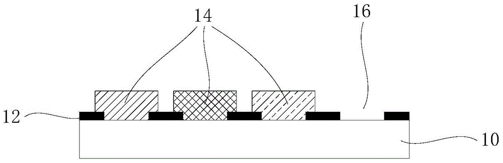
[0022] Figure 1A to Figure 1E is a schematic diagram of the manufacturing method of the color filter substrate according to the first embodiment of the present invention. In the first embodiment, the display mode of the liquid crystal display panel with the color filter substrate may be, for example, a vertical alignment (VA) mode or a twisted nematic (TN) display mode.

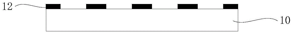
[0023] First, please refer to Figure 1A , providing a substrate 10, such as an insulating transparent substrate, which is defined as a color filter substrate, usually referred to as an upper substrate; then, a black matrix (black matrix) light-shielding portion 12 is formed on the substrate 10, wherein the black The material of the matrix light-shielding part 12 can be black resin or metal chromium, for example, a black resin with a certain thickness is made by a yellow light process, preferably a polymer material mixed with acrylic and carbon, or a certain thickness is also made by a yellow light process. ...

no. 2 example

[0029] In the second embodiment according to the present invention, the method before forming the spacer 24 is the same as that of the first embodiment, that is, the method before forming the spacer 24 in the second embodiment can refer to Figure 1A to Figure 1D . Here, to avoid redundant description, only the differences from the method of forming the spacers 24 in the first embodiment are described in the second embodiment.

[0030] First of all, it should be noted that the display mode of the liquid crystal display panel with the color filter substrate of the second embodiment may be, for example, a fringe field switching (FFS) mode or an in-plane switching (IPS) display mode.

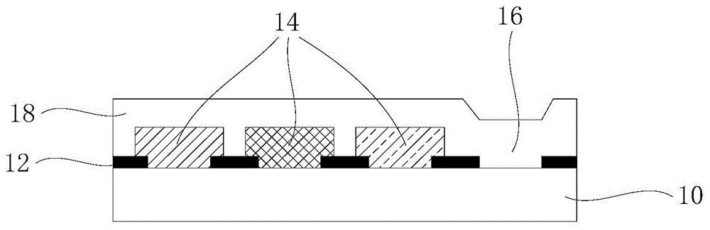
[0031] figure 2 is a schematic diagram of a spacer forming method according to a second embodiment of the present invention.

[0032] refer to figure 2 After the surface of the transparent photoresist layer 18 is flat, it is beneficial to subsequently deposit the electrode layer 22 on the tran...


PUM


Abstract

The invention discloses a method for manufacturing a color filter substrate. The method comprises the following steps of providing a substrate (10); forming a light shielding portion (12) on the substrate (10); forming a color filter, which comprises a colorful portion (14) and an opening portion (16), on the substrate (10); covering the substrate (10) by using a flat layer (18) which is filled in the opening portion (16); photoetching the flat layer (18); and forming a spacer (24) on the photoetched flat layer (18). A transparent light resistance layer is filled in the opening portion and serves as a white light resistor, and the surface of the transparent light resistance layer is flattened by using a photoetching technology. Compared with the prior art, the method for manufacturing the color filter substrate has the advantages that a white color resistor photoetching manufacture procedure is omitted, the transparent light resistance layer on the opening portion cannot be sunken, irregularity of the surface of the transparent light resistance layer is avoided, and the display quality of a manufactured liquid crystal display panel is improved.

Description

technical field [0001] The invention relates to a method for manufacturing a color filter substrate, in particular to a method for manufacturing a color filter substrate in which the surface of a flat layer is flattened by photolithography. Background technique [0002] The liquid crystal display panel includes an upper substrate and a lower substrate facing each other, and a liquid crystal layer sandwiched between the upper and lower substrates. The upper substrate is usually called a color filter (Color Filter, CF) substrate, and the lower substrate is usually called an array (Array) substrate. With the development of information technology, various requirements for liquid crystal display panels are also increasing, among which, high transmittance, low power consumption, and good image quality have become people's requirements for display panels. In order to meet these needs, a liquid crystal display panel consisting of red (R) sub-pixels, green (G) sub-pixels, blue (B) s...

Claims


Application Information

Patent Timeline
Patent Type & Authority Applications(China)
IPC IPC(8): G02F1/1335G02B5/20G03F7/00
CPCG02F1/133514G02F1/133516G02F1/133512G03F7/0007G02B5/22G02B5/201G02F1/133519G02B5/20G03F7/70283G03F7/16G03F7/20G03F7/32
Inventor 薛景峰陈归
Owner TCL CHINA STAR OPTOELECTRONICS TECH CO LTD
Why Eureka
Try Eureka